Data Sheet AD8145
APPLICATIONS INFORMATION
OVERVIEW
The AD8145 contains three independent active feedback
amplifiers that can be effectively applied as differential line
receivers for red-green-blue (RGB) signals or component video
signals, such as YPbPr, transmitted over UTP cable. The AD8145
also contains two general-purpose comparators with hysteresis
that can be used to receive digital signals or to extract video
synchronization pulses from received common-mode signals
that contain encoded synchronization signals.
The comparators, which receive power from the positive supply, are
referenced to GND and require greater than 4.5 V on the positive
supply for proper operation. If the comparators are not used,
then a split ±2.5 V can be used with the amplifiers operating
normally.
The AD8145 includes a power-down feature that can be asserted to
reduce the supply current when a particular device is not in use.
BASIC CLOSED-LOOP GAIN CONFIGURATIONS
Each amplifier in the AD8145 comprises two transconductance
amplifiers—one for the input signal and one for negative feedback.
Note that the closed-loop gain of the amplifier used in the signal
path is defined as the single-ended output voltage of the amplifier
divided by its differential input voltage. Therefore, each amplifier
in the AD8145 provides differential-to-single-ended gain.
Additionally, the amplifier used for feedback has two high
impedance inputsthe feedback input, where the negative
feedback is applied, and the REF input, that can be used as
an independent single-ended input to apply a dc offset to the
output signal.
The AD8145 contains on-chip feedback networks between each
amplifier output and its respective feedback input. The closed-
loop gain of the amplifier is set to 1 by connecting the amplifier
output directly to its respective GAIN_x pin. Doing this places
the on-chip resistors and capacitor in parallel across the amplifier
output and feedback pin. The small feedback capacitor mitigates
the effects of the summing-node capacitance, which is most
problematic in the unity gain case. Closed-loop gain of an
amplifier is set to 2 by connecting the respective GAIN_x pin
to a reference voltage, often directly to ground. In Figure 1,
R = 350 Ω and C = 2 pF.
Some basic gain configurations implemented with an AD8145
amplifier are shown in Figure 33 through Figure 36.
GAIN
REF
R
R
0.01µF
0.01µF
+5V
–5V
C
OUT
V
OUT
V
IN
V
REF
06307-034
Figure 33. Basic Gain = 1 Circuit: V
OUT
= V
IN
+ V
REF
The gain equation for the circuit in Figure 33 is
V
OUT
= V
IN
+ V
REF
(1)
In this configuration, the voltage applied to the REF pin appears
at the output with a gain of 1.
Figure 34 illustrates one way to operate an AD8145 amplifier
with a gain of 2.
GAIN
REF
RR
0.01µF
0.01µF
+5V
–5V
C
V
REF
V
OUT
V
IN
06307-035
Figure 34. Basic Gain = 2 Circuit: V
OUT
= 2(V
IN
+ V
REF
)
The gain equation for the circuit in Figure 34 is
V
OUT
= 2(V
IN
+ V
REF
) (2)
Rev. B | Page 15 of 21
AD8145 Data Sheet
To achieve unity gain from V
REF
to V
OUT
in this configuration,
divide V
REF
by the same factor used in the feedback loop; the
divider resistors, R
D
, need not be the same values used in the
internal feedback loop. Figure 35 illustrates this approach.
GAIN
REF
R
R
0.01µF
0.01µF
+5V
–5V
C
V
REF
V
OUT
V
IN
R
D
R
D
06307-036
Figure 35. Basic Gain Circuit: V
OUT
= 2V
IN
+ V
REF
The gain equation for the circuit in Figure 35 is
V
OUT
= 2V
IN
+ V
REF
(3)
Another configuration that provides the same gain equation as
Equation 3 is shown in Figure 36. In this configuration, it is
important to keep the source resistance of V
REF
much smaller
than 350 Ω to avoid gain errors.
GAIN
REF
RR
0.01µF
0.01µF
+5V
–5V
C
V
REF
V
OUT
V
IN
06307-037
Figure 36. Basic Gain Circuit: V
OUT
= 2V
IN
+ V
REF
For stability reasons, the inductance of the trace connected to
the REF_x pin must be kept to less than 10 nH. The typical
inductance of 50 Ω traces on the outer layers of the FR-4 boards
is 7 nH/in, and on the inner layers, it is typically 9 nH/in. Vias
must be accounted for as well. The inductance of a typical via in
a 0.062-inch board is 1.5 nH. If longer traces are required, a 200
resistor should be placed in series with the trace to reduce the
Q-factor of the inductance.
In many dual-supply applications, V
REF
can be directly connected to
ground right at the device.
TERMINATING THE INPUT
One of the key benefits of the active feedback architecture is the
separation that exists between the differential input signal and
the feedback network. Because of this separation, the differential
input maintains its high CMRR and provides high differential
and common-mode input impedances, making line termination
a simple task.
Most applications that use the AD8145 involve transmitting broad-
band video signals over 100 Ω UTP cables and use dc-coupled
terminations. The two most common types of dc-coupled
terminations are differential and common-mode. Differential
termination of 100 Ω UTP cables is implemented by simply
connecting a 100 Ω resistor across the amplifier input, as shown
in Figure 37.
GAIN
REF
R
R
0.01µF
0.01µF
+5V
–5V
C
OUT
V
OUT
V
IN
100Ω
UTP
100Ω
06307-038
Figure 37. Differential-Mode Termination with G = 1
Some applications require common-mode terminations for
common-mode currents generated at the transmitter. In these
cases, the 100 Ω termination resistor is split into two 50 Ω
resistors. The required common-mode termination voltage is
applied at the tap between the two resistors. In many of these
applications, the common-mode tap is connected to ground
(V
TERM
(CM) = 0). This scheme is illustrated in Figure 38.
GAIN
REF
R
R
0.01µF
0.01µF
+5V
–5V
C
OUT
V
OUT
V
IN
100Ω
UTP
50Ω
50Ω
V
TERM
(CM)
06307-039
Figure 38. Common-Mode Termination with G = 1
Rev. B | Page 16 of 21
Data Sheet AD8145
INPUT CLAMPING
The differential input that is assigned to receive the input signal
includes clamping diodes that limit the differential input swing
to approximately 5.5 V p-p at 25°C. Because of this, the input
and feedback stages should never be interchanged.
The supply current drawn by the AD8145 has a strong dependence
on the input signal magnitude because the input transconductance
stages operate with differential input signals that can be up to a
few volts peak-to-peak. This behavior is distinctly different
from that of traditional op amps, where the differential input
signal is driven to essentially 0 V by negative feedback.
For most applications, including receiving RGB video signals,
the input signal magnitudes encountered are well within the
safe operating limits of the AD8145 over its full power supply
and operating temperature ranges. In some extreme applications
where large differential and/or common-mode voltages are
encountered, external clamping may be necessary. External
common-mode clamping is also sometimes required when an
unpowered AD8145 receives a signal from an active driver. In
this case, external diodes are required when the current drawn
by the internal ESD diodes cannot be kept to less than 5 mA.
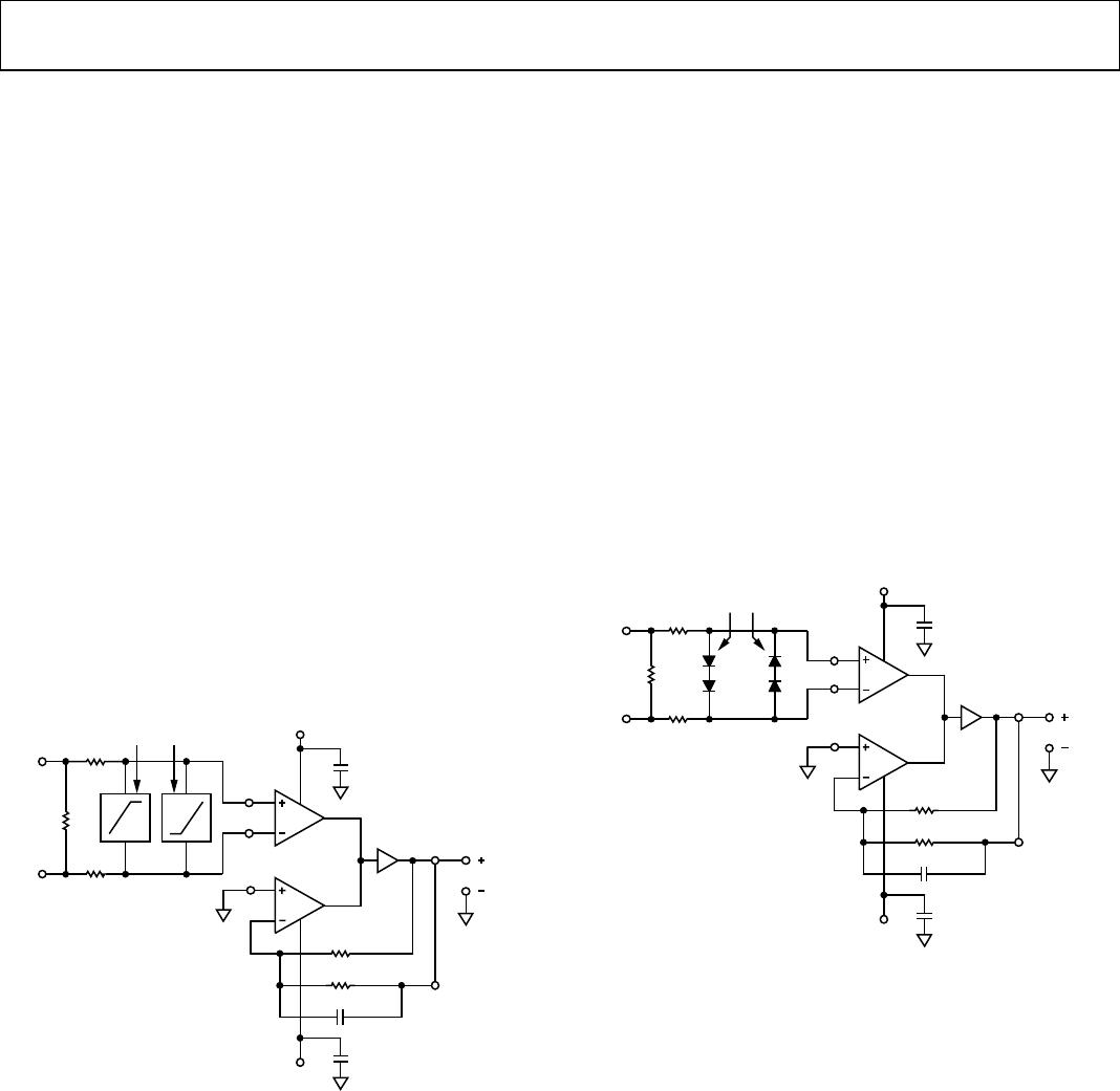
Figure 39 shows a general approach to external differential-mode
clamping.
POSITIVE CLAMP NEGATIVE CLAMP
R
S
R
T
V
IN
R
S
+
GAIN
REF
R
R
0.01µF
0.01µF
+5V
–5V
C
OUT
V
OUT
06307-040
Figure 39. Differential-Mode Clamping with G = 1
The positive and negative clamps are nonlinear devices that exhibit
very low impedance when the voltage across them reaches a
critical threshold (clamping voltage), thereby limiting the voltage
across the AD8145 input. The positive clamp has a positive
threshold, and the negative clamp has a negative threshold.
A diode is a simple example of such a clamp. Schottky diodes
generally have lower clamping voltages than typical signal diodes.
The clamping voltage should be larger than the largest expected
signal amplitude, with enough margin to ensure that the received
signal passes without being distorted.
A simple way to implement a clamp is to use a number of diodes in
series. The resultant clamping voltage is then the sum of the
clamping voltages of individual diodes.
A 1N4448 diode has a forward voltage of approximately 0.70 V
to 0.75 V at typical current levels that are seen when it is being
used as a clamp, and 2 pF maximum capacitance at 0 V bias.
(The capacitance of a diode decreases as its reverse-bias voltage
is increased.) The series connection of two 1N4448 diodes,
therefore, has a clamping voltage of 1.4 V to 1.5 V. Figure 40
shows how to limit the differential input voltage applied to an
AD8145 amplifier to ±1.4 V to ±1.5 V (2.8 V p-p to 3.0 V p-p).
Note that the capacitance of the two series diodes is half that of
one diode. Different numbers of series diodes can be used to
obtain different clamping voltages.
R
T
is the differential termination resistor, and the series
resistances, R
S
, limit the current into the diodes. The series
resistors should be highly matched in value to preserve high
frequency CMRR.
POSITIVE CLAMP NEGATIVE CLAMP
R
S
R
T
V
IN
R
S
+
GAIN
REF
R
R
0.01µF
0.01µF
+5V
–5V
C
OUT
V
OUT
06307-041
Figure 40. Using Two 1N4448 Diodes in Series as a Clamp
Many other nonlinear devices can be used as clamps. The best
choice for a particular application depends upon the desired
clamping voltage, response time, parasitic capacitance, and
other factors.
When using external differential-mode clamping, it is important
to ensure that the series resistors (R
S
), the sum of the parasitic
capacitance of the clamping devices, and the input capacitance
of the AD8145 are small enough to preserve the desired signal
bandwidth.
Rev. B | Page 17 of 21

AD8145WYCPZ-R7

Mfr. #:
Manufacturer:
Analog Devices Inc.
Description:
Video Amplifiers Hi Spd Trple Diff Rcvr w/ Comparator
Lifecycle:
New from this manufacturer.
Delivery:
DHL FedEx Ups TNT EMS
Payment:
T/T Paypal Visa MoneyGram Western Union

Products related to this Datasheet