EVAL-AD5420EBZ

UG-441 Evaluation Board User Guide
Rev. D | Page 4 of 12
Table 4. Link Options
Link No. Description
LK1 Not applicable.
LK2 This link selects the state of the CLEAR pin (when the evaluation board is configured for external control).
Position A ties the CLEAR pin to 0 V.
Position B ties the CLEAR pin to DV
CC.
LK3 This link selects the state of the DV
CC
SELECT pin.
When this link is inserted, the DV
CC
SELECT pin is tied to 0 V, disabling the internal supply; an external supply must be
connected to the DV
CC
pin via LK17.
When this link is removed, the DV
CC
SELECT pin is unconnected, enabling the internal supply. Removing the requirement for
an external digital supply, LK17 can be removed.
LK4 Not applicable.
LK5
This link selects how the I
OUT
current loop return is connected to ground on the evaluation board.
Position A connects the I
OUT
current loop return directly to ground.
Position B connects the I
OUT
current loop return input to GND through a 51 Ω resistor. The high side of the resistor is
connected to the V
IN
1 input of the on-board ADC, allowing readback to the PC of the output current.
LK6 This link selects the 5 V power supply source for the digital circuitry.
Position A selects the USB port as the 5 V digital circuitry power supply source.
Position B selects J7 as the 5 V digital circuitry power supply source.
LK7 This link selects whether the AD5420 evaluation board is controlled by the PC via the USB port or by an external source via J8.
Position A selects the evaluation board to be controlled by the PC via the USB port.
Position B selects the evaluation board to be controlled by an external source via J8.
LK8 This link selects the digital supply voltage value for the AD5420 and the on-board ADC (U6).
Position A selects 5 V as the supply value.
Position B selects 3.3 V as the supply value.
LK9 This link selects the positive power supply source for U2 and U6.
Position A selects the AV
DD
input as the positive power supply source (use only if the power supply applied to AV
DD
is less
than 16.5 V).
Position B selects the V+ input as the positive power supply source (use if the power supply applied to AV
DD
input is greater
than 16.5 V). A power supply voltage of 10.8 V to 16.5 V can be applied to V+.
LK10 This link is used to enable/disable the external boost transistor.
When this link is inserted, the external boost transistor is disabled.
When this link is removed, the external boost transistor is enabled.
LK11 Not applicable.
LK12 Not applicable.
LK13 This link connects the I
OUT
connector directly to the GND connector.
When this link is inserted, the I
OUT
connector is connected directly to the GND connector.
When this link is removed, the I
OUT
connector is disconnected from the GND connector (an external load must be connected).
LK14 Not applicable.
LK15
This link selects the voltage reference source.
Position A selects the internal voltage reference of the AD5420 as the voltage reference source.
Position B selects an external source that can be applied at Connector J3.
Position C selects the on-board ADR435 as the voltage reference source.
LK16 Not applicable.
LK17 This link connects the DV
CC
pin of the AD5420 to the on-board digital power supply.
When this link is inserted, the DV
CC
pin of the AD5420 is connected to the on-board digital power supply (LK3 must be
inserted to disable the AD5420 internal digital power supply).
When this link is removed, the DV
CC
pin of the AD5420 is disconnected from the on-board digital power supply (LK3 should
be removed to enable the AD5420 internal digital power supply).
LK18 This link connects the AV
DD
pin of the AD5420 to the power supply applied at the AV
DD
input connector, J2 (LK18 must be
inserted for operation of the AD5420).
Evaluation Board User Guide UG-441
Rev. D | Page 5 of 12
EVALUATION BOARD SOFTWARE
SOFTWARE INSTALLATION
The AD5420 evaluation kit includes self-installing software on a
CD. The software is compatible with Windows 2000/NT/XP. If
the setup file does not run automatically, run the setup.exe file
from the CD.
To install the evaluation software, do the following:
1. Install the evaluation software before connecting the
evaluation board to the USB port of the PC to ensure that
the evaluation board is correctly recognized when connected
to the PC.
2. After installation from the CD is complete, power up the
AD5420 evaluation board as described in the Power Supplies
section.
3. Connect the board to the USB port of the PC using the
supplied cable.
4. When the evaluation board is detected, proceed through
any dialog boxes that appear. This finishes the installation.
SOFTWARE OPERATION
To launch the software, complete the following steps:
1. From the Start menu, select Analog Devices AD5420/
AD5420 Evaluation Software. The main window of the
software then displays (see Figure 3).
2. If the evaluation board is not connected to the USB port
when the software is launched, a connectivity error is
displayed (see Figure 2). Simply connect the evaluation
board to the USB port of the PC and click Retr y.
08160-002
Figure 2. Connectivity Error Alert
Figure 3. Main Window
UG-441 Evaluation Board User Guide
Rev. D | Page 6 of 12
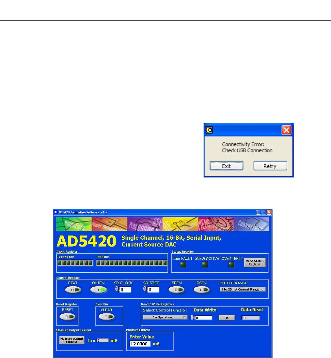
The main window is divided into eight sections: Input Register,
Status Register, Control Register, Reset Register, Clear Pin,
Read/Write Registers, Measure Output Current, and
Program Current.
Input Register
The Input Register section displays the contents of the input
register. The 24-bit display is updated each time a read or a
write operation is requested via the main window controls. It
allows users to associate the value written to the AD5420 with
the various programmable functions.
Status Register
The Status Register section displays the states of the three bits
of the read-only status register. To read the register, click the
Read Status Register button.
Control Register
The Control Register section facilitates programming of the
control register on an individual bit basis. To change the value
of a bit, click the relevant button. Each button also displays the
current state of the bit. You can also enter code in the SR CLOCK
and SR STEP text boxes and select an output range from the
OUTPUT RANGE drop-down box.
When using an external current setting resistor, it is recom-
mended to only set REXT when also setting the OUTEN bit.
Alternately, REXT can be set before the OUTEN bit is set, but
the range must be changed on the write in which the output is
enabled. The Read/Write Registers section should be used for
these commands (see Figure 4).
Reset Register
The sole function of the Reset Register section is to allow the
AD5420 to be reset to its power-on state. To change the value of
the reset bit, click the RESET button.
CLEAR Pin
In the Clear Pin section, you can change the state of the CLEAR
pin by clicking the CLEAR button.
Read/Write Registers
In the Read/Write Registers section, you can read and write to
all registers in the AD5420. To select a register and request a read
or write, click the Select Control Function box. Then, to write
data to the register, click the Data Write button until the desired
data is displayed in the Data Write text box and then click OK.
Register data is updated and displayed for you to read in the
Data Read text box each time you click OK.
Measure Output Current
To display the programmed output current in the Measure Output
Current section, click the Measure output Current button.
The output current is measured using the on-board ADC and
is displayed in milliamperes (mA) in the I
OUT
box. The output
current is measured with an accuracy of approximately 1% and is
not intended as precise, but rather as an approximate, feedback
of the programmed current.
Program Current
To program a current output value, enter the value in milli-
amperes (mA) in the Enter Value text box of the Program Current
section, and press Enter. The output must first be enabled, and
the output range must be selected via the Control Register section.
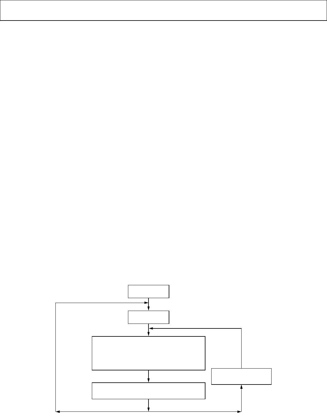
08160-300
POWER-ON
SOFTWARE RESET
CONTROL REGISTER WRITE (ONE WRITE COMMAND)
• SELECT R
SET
EXTERNAL/INTERNAL
• SET THE REQUIRED RANGE
• CONFIGURE THE SLEW RATE CONTROL (IF REQUIRED)
• CONFIGURE DAISY CHAIN MODE (IF REQUIRED)
• ENABLE THE OUTPUT
DATA REGISTER WRITE
• WRITE REQUIRED CODE TO DATA REGISTER
CONTROL REGISTER WRITE
• DISABLE OUTPUT
R
SET
CONFIGURATION CHANGE RANGE CHANGE
Figure 4. Programming Sequence to Write/Enable the Output Correctly

EVAL-AD5420EBZ

Mfr. #:
Manufacturer:
Analog Devices Inc.
Description:
Data Conversion IC Development Tools EVAL BRD AD5420
Lifecycle:
New from this manufacturer.
Delivery:
DHL FedEx Ups TNT EMS
Payment:
T/T Paypal Visa MoneyGram Western Union

Products related to this Datasheet