NXP Semiconductors
PBHV9115TLH
150 V, 1 A PNP high-voltage low VCEsat BISS transistor
PBHV9115TLH All information provided in this document is subject to legal disclaimers.
©
NXP Semiconductors N.V. 2017. All rights reserved
Product data sheet 16 January 2017 3 / 14
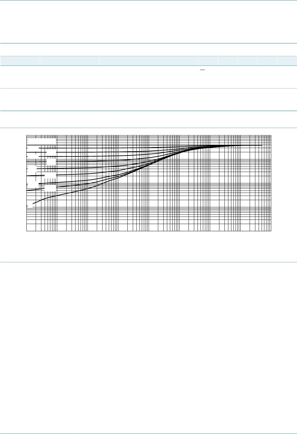
8. Limiting values
Table 5. Limiting values
In accordance with the Absolute Maximum Rating System (IEC 60134).
Symbol Parameter Conditions Min Max Unit
V
CBO
collector-base voltage open emitter - -200 V
V
CEO
collector-emitter voltage open base - -150 V
V
CESM
collector-emitter peak
voltage
V
BE
= 0 V - -200 V
V
EBO
emitter-base voltage open collector - -6 V
I
C
collector current - -1 A
I
CM
peak collector current - -2 A
I
BM
peak base current
single pulse; t
p
≤ 1 ms
- -400 mA
P
tot
total power dissipation T
amb
≤ 25 °C
[1]
- 300 mW
T
j
junction temperature - 150 °C
T
amb
ambient temperature -55 150 °C
T
stg
storage temperature -65 150 °C
[1] Device mounted on an FR4 PCB, single-sided copper, tin-plated and standard footprint.
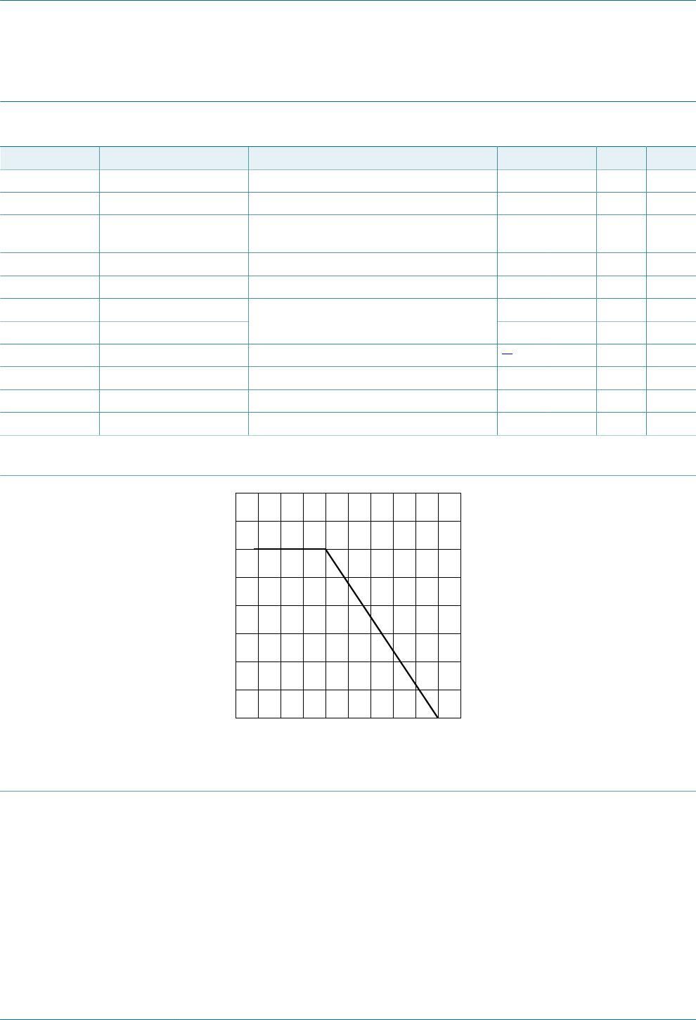
T
amb
(°C)
- 75 17512525 75- 25
006aab150
200
100
300
400
P
tot
(mW)
0
FR4 PCB, standard footprint
Fig. 1. Power derating curve