ZL30136 Short Form Data Sheet
3
Zarlink Semiconductor Inc.
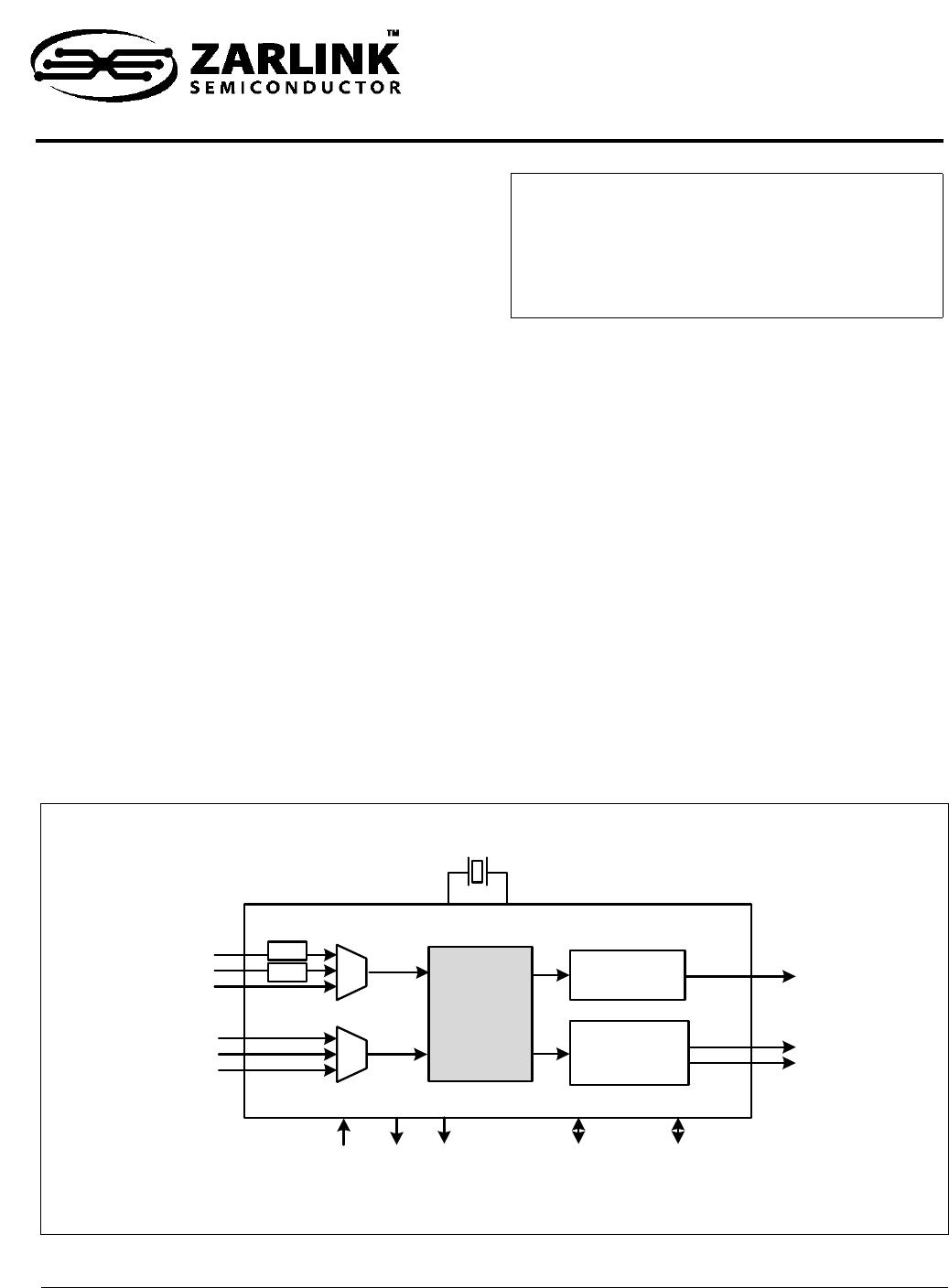
Pin Description
Pin # Name
I/O
Type
Description
Input Reference
B1
A3
B4
ref0
ref1
ref2
I
u
Input References 2:0 (LVCMOS, Schmitt Trigger). These input references are
available to the DPLL for synchronizing output clocks. All three input references
can lock to 2 kHz or any multiple of 8 kHz up to 77.76 MHz including 25 MHz and
50 MHz. Input ref0 and ref1 have additional configurable pre-dividers allowing
input frequencies of 62.5 MHz, 125 MHz, and 155.52 MHz. These pins are
internally pulled up to V
dd
.
A1
A2
A4
sync0
sync1
sync2
I
u
Frame Pulse Synchronization References 2:0 (LVCMOS, Schmitt Trigger).
These are optional frame pulse synchronization inputs associated with input
references 0, 1 and 2. These inputs accept frame pulses in a clock format (50%
duty cycle) or a basic frame pulse format with minimum pulse width of 5 ns.
These pins are internally pulled up to V
dd.
Output Clocks and Frame Pulses
D8 eth_clk O Network Output Clock (LVCMOS). This output can be configured to provide
any of the Ethernet clock rates: 12.5 MHz, 25 MHz, 50 MHz, 62.5 MHz, or
125 MHz.
G8 p_clk O Programmable Telecom Synthesizer - Output Clock (LVCMOS). This output
can be configured to provide telecom clock rates in multiples of 8 kHz up to
100 MHz. The default frequency for this output is 2.048 MHz.
G7 p_fp O Programmable Telecom Synthesizer - Output Frame Pulse (LVCMOS). This
output can be configured to provide virtually any style of output frame pulse. The
default frequency for this frame pulse output is 8 kHz.
Control
G5 rst_b I Reset (LVCMOS, Schmitt Trigger). A logic low at this input resets the device. To
ensure proper operation, the device must be reset after power-up. Reset should
be asserted for a minimum of 300 ns.
B2 mode I
u
DPLL Mode Select (LVCMOS, Schmitt Trigger). During reset, the level on this
pin determines the default mode of operation for DPLL (Normal=0 or Freerun=1).
After reset, the mode of operation can be controlled directly with this pin, or by
accessing the dpll_modesel register (0x1F) through the serial interface. This pin
is internally pulled up to Vdd.
Status
E1 lock O Lock Indicator (LVCMOS). This is the lock indicator pin for DPLL. This output
goes high when the DPLL’s output is frequency and phase locked to the input
reference.
H1 hold O Holdover Indicator (LVCMOS). This pin goes high when the DPLL enters the
holdover mode.
Serial Interface (SPI/I
2
C)
C1 sck/scl I/B Clock for Serial Interface (LVCMOS). Serial interface clock. When i2c_en = 0,
this pin acts as the sck pin for the serial interface. When i2c_en = 1, this pin acts
as the scl pin (bidirectional) for the I
2
C interface.