45
COMMERCIAL AND INDUSTRIAL
TEMPERATURE RANGES
IDT72V3640/50/60/70/80/90 3.3V HIGH DENSITY SUPERSYNC II
TM
36-BIT FIFO
1,024 x 36, 2,048 x 36, 4,096 x 36, 8,192 x 36, 16,384 x 36 and 32,768 x 36
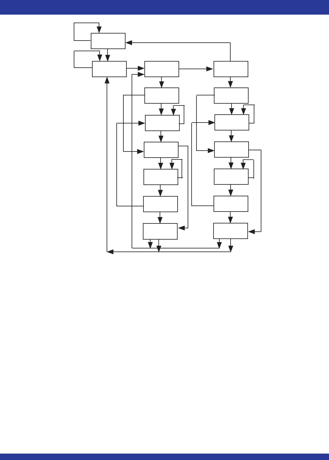
THE INSTRUCTION REGISTER
The Instruction register allows an instruction to be shifted in serially into the
processor at the rising edge of TCLK.
The Instruction is used to select the test to be performed, or the test data
register to be accessed, or both. The instruction shifted into the register is latched
at the completion of the shifting process when the TAP controller is at Update-
IR state.
The instruction register must contain 4 bit instruction register-based cells
which can hold instruction data. These mandatory cells are located nearest the
serial outputs they are the least significant bits.
TEST DATA REGISTER
The Test Data register contains three test data registers: the Bypass, the
Boundary Scan register and Device ID register.
These registers are connected in parallel between a common serial input
and a common serial data output.
The following sections provide a brief description of each element. For a
complete description, refer to the IEEE Standard Test Access Port Specification
(IEEE Std. 1149.1-1990).
TEST BYPASS REGISTER
The register is used to allow test data to flow through the device from TDI
to TDO. It contains a single stage shift register for a minimum length in serial path.
When the bypass register is selected by an instruction, the shift register stage
is set to a logic zero on the rising edge of TCLK when the TAP controller is in
the Capture-DR state.
The operation of the bypass register should not have any effect on the
operation of the device in response to the BYPASS instruction.
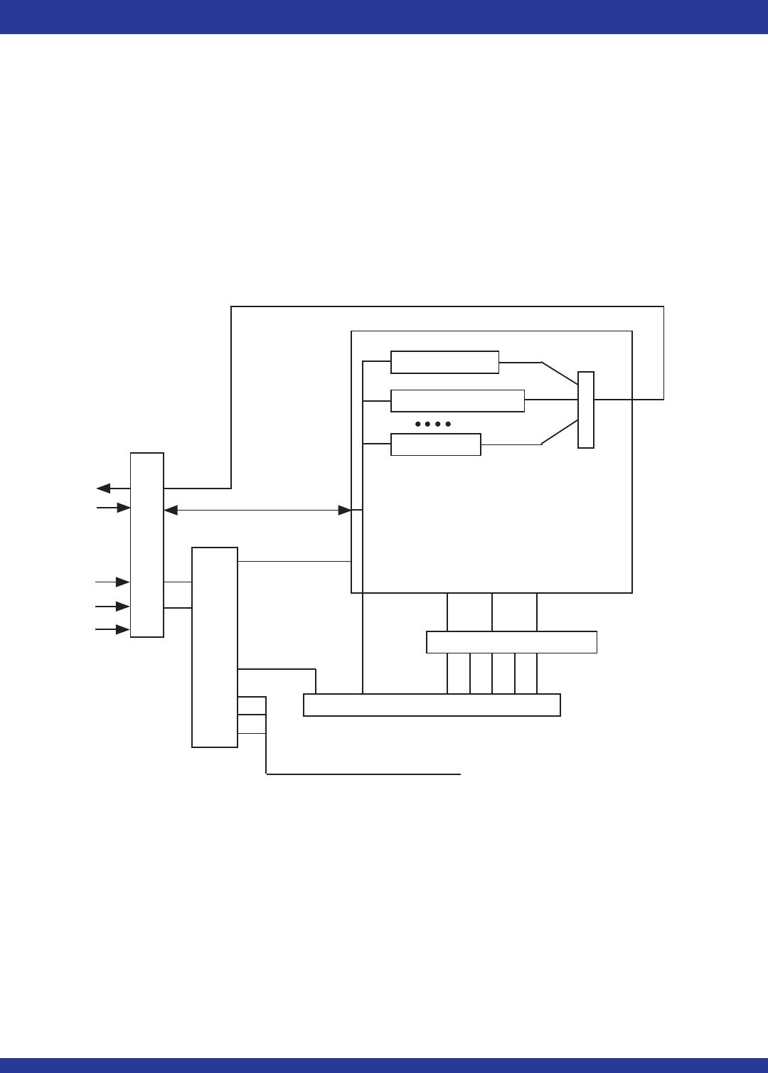
THE BOUNDARY-SCAN REGISTER
The Boundary Scan Register allows serial data TDI be loaded in to or read
out of the processor input/output ports. The Boundary Scan Register is a part
of the IEEE 1149.1-1990 Standard JTAG Implementation.
THE DEVICE IDENTIFICATION REGISTER
The Device Identification Register is a Read Only 32-bit register used to
specify the manufacturer, part number and version of the processor to be
determined through the TAP in response to the IDCODE instruction.
IDT JEDEC ID number is 0xB3. This translates to 0x33 when the parity
is dropped in the 11-bit Manufacturer ID field.
For the IDT72V3640/72V3650/72V3660/72V3670/72V3680/72V3690,
the Part Number field contains the following values:
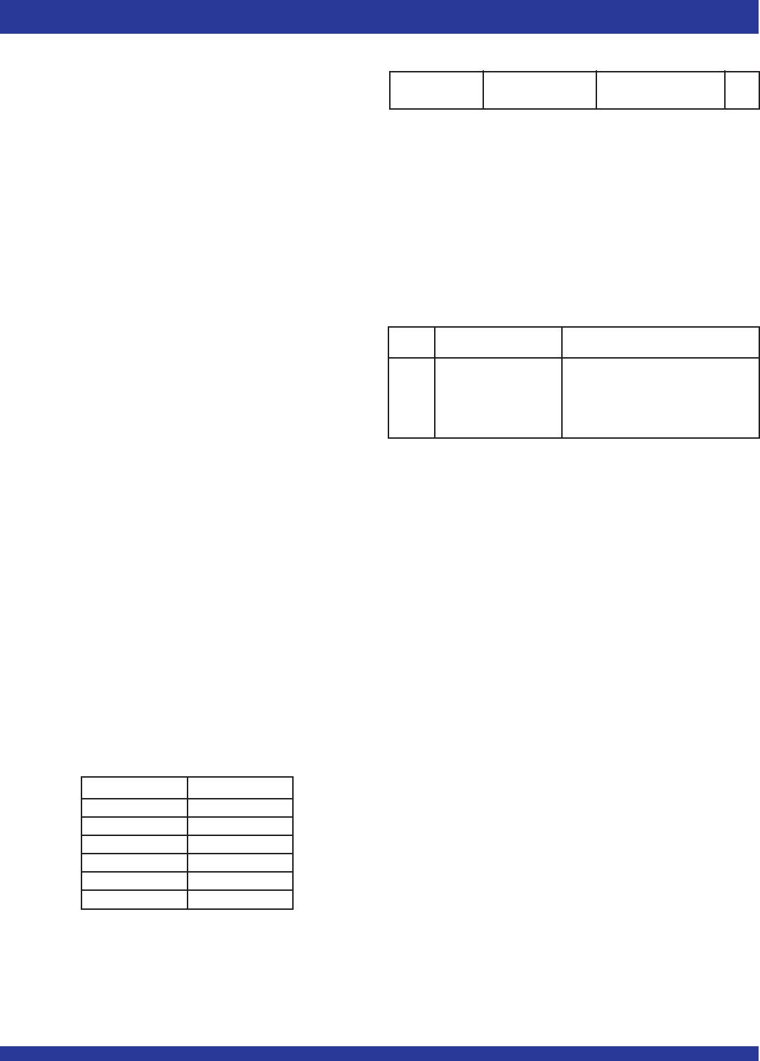
IDT72V3640/50/60/70/80/90 JTAG Device Identification Register
31(MSB) 28 27 12 11 1 0(LSB)
Version (4 bits) Part Number (16-bit) Manufacturer ID (11-bit)
0X0 0X33 1
JTAG INSTRUCTION REGISTER
The Instruction register allows instruction to be serially input into the device
when the TAP controller is in the Shift-IR state. The instruction is decoded to
perform the following:
• Select test data registers that may operate while the instruction is
current. The other test data registers should not interfere with chip
operation and the selected data register.
• Define the serial test data register path that is used to shift data between
TDI and TDO during data register scanning.
The Instruction Register is a 4 bit field (i.e.IR3, IR2, IR1, IR0) to decode 16
different possible instructions. Instructions are decoded as follows.
Hex Instruction Function
Value
0x00 EXTEST Select Boundary Scan Register
0x02 IDCODE Select Chip Identification data register
0x01 SAMPLE/PRELOAD Select Boundary Scan Register
0x03 HI-Z JTAG
0x0F BYPASS Select Bypass Register
Table 6. JTAG Instruction Register Decoding
The following sections provide a brief description of each instruction. For
a complete description refer to the IEEE Standard Test Access Port Specification
(IEEE Std. 1149.1-1990).
EXTEST
The mandatory EXTEST instruction is provided for external circuity and
board level interconnection check.
IDCODE
This instruction is provided to select Device Identification Register to read
out manufacture’s identity, part number and version number.
SAMPLE/PRELOAD
The mandatory SAMPLE/PRELOAD instruction allows data values to be
loaded onto the latched parallel outputs of the boundary-scan shift register prior
to selection of the boundary-scan test instruction. The SAMPLE instruction
allows a snapshot of data flowing from the system pins to the on-chip logic or vice
versa.
HIGH-Z
This instruction places all the output pins on the device into a high impedance
state.
BYPASS
The Bypass instruction contains a single shift-register stage and is set to
provide a minimum-length serial path between the TDI and the TDO pins of the
device when no test operation of the device is required.
Device Part# Field
IDT72V3640 04E5
IDT72V3650 04E4
IDT72V3660 04E3
IDT72V3670 04E2
IDT72V3680 04E1
IDT72V3690 04E0