8
COMMERCIAL AND INDUSTRIAL
TEMPERATURE RANGES
IDT72V3640/50/60/70/80/90 3.3V HIGH DENSITY SUPERSYNC II
TM
36-BIT FIFO
1,024 x 36, 2,048 x 36, 4,096 x 36, 8,192 x 36, 16,384 x 36 and 32,768 x 36
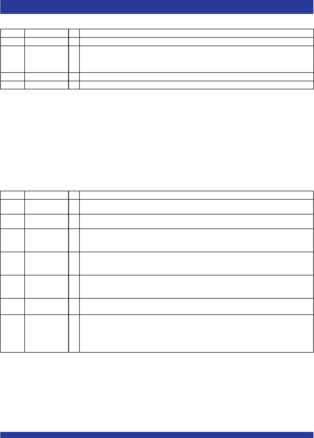
ABSOLUTE MAXIMUM RATINGS
Symbol Rating Com’l & Ind’l Unit
V
TERM
(2)
Terminal Voltage –0.5 to +4.5 V
with respect to GND
T
STG Storage –55 to +125 °C
Temperature
I
OUT DC Output Current –50 to +50 mA
NOTES:
1. Stresses greater than those listed under ABSOLUTE MAXIMUM RATINGS may cause
permanent damage to the device. This is a stress rating only and functional operation of
the device at these or any other conditions above those indicated in the operational
sections of this specification is not implied. Exposure to absolute maximum rating
conditions for extended periods may affect reliability.
2. V
CC terminal only.
NOTES:
1. With output deselected, (OE ≥ V
IH).
2. Characterized values, not currently tested.
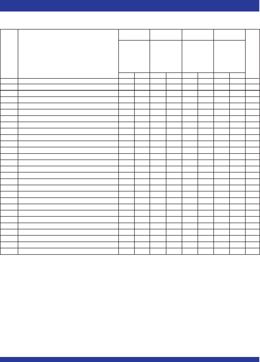
DC ELECTRICAL CHARACTERISTICS
(Commercial: VCC = 3.3V ± 0.15V, TA = 0°C to +70°C;Industrial: VCC = 3.3V ± 0.15V, TA = -40°C to +85°C; JEDEC JESD8-A compliant)
CAPACITANCE (TA = +25°C, f = 1.0MHz)
Symbol Parameter
(1)
Conditions Max. Unit
CIN
(2)
Input VIN = 0V 10 pF
Capacitance
C
OUT
(1,2)
Output VOUT = 0V 10 pF
Capacitance
Symbol Parameter Min. Typ. Max. Unit
VCC
(1)
Supply Voltage Com’l/Ind’l 3.15 3.3 3.45 V
GND Supply Voltage Com’l/Ind’l 0 0 0 V
V
IH
(2)
Input High Voltage Com’l/Ind’l 2.0 — 5.5 V
V
IL
(3)
Input Low Voltage Com’l/Ind’l — — 0.8 V
TA Operating Temperature 0 — 70 °C
Commercial
T
A Operating Temperature -40 — 85 °C
Industrial
NOTES:
1. VCC = 3.3V ± 0.15V, JEDEC JESD8-A compliant.
2. Outputs are not 5V tolerant.
3. 1.5V undershoots are allowed for 10ns once per cycle.
IDT72V3640L
IDT72V3650L
IDT72V3660L
IDT72V3670L
IDT72V3680L
IDT72V3690L
Commercial and Industrial
(1)
tCLK = 6, 7-5, 10, 15 ns
Symbol Parameter Min. Max. Unit
ILI
(2)
Input Leakage Current –1 1 μA
ILO
(3)
Output Leakage Current –10 10 μA
VOH Output Logic “1” Voltage, IOH = –2 mA 2.4 — V
VOL Output Logic “0” Voltage, IOL = 8 mA — 0.4 V
ICC1
(4,5,6)
Active Power Supply Current — 40 mA
I
CC2
(4,7)
Standby Current — 15 mA
NOTES:
1. Industrial temperature range product for the 7-5ns and 15ns speed grades are available as a standard device. All other speed grades are available by special order.
2. Measurements with 0.4 ≤ VIN ≤ VCC.
3. OE ≥ VIH, 0.4 ≤ VOUT ≤ VCC.
4. Tested with outputs open (IOUT = 0).
5. RCLK and WCLK toggle at 20 MHz and data inputs switch at 10 MHz.
6. Typical ICC1 = 4.2 + 1.4*fS + 0.002*CL*fS (in mA) with VCC = 3.3V, tA = 25°C, fS = WCLK frequency = RCLK frequency (in MHz, using TTL levels), data switching at fS/2,
CL = capacitive load (in pF).
7. All Inputs = VCC - 0.2V or GND + 0.2V, except RCLK and WCLK, which toggle at 20 MHz.
RECOMMENDED DC OPERATING
CONDITIONS