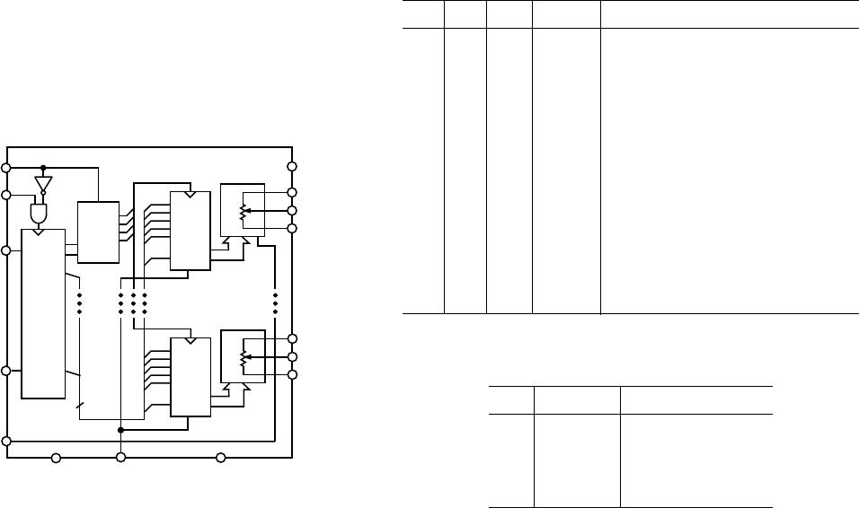
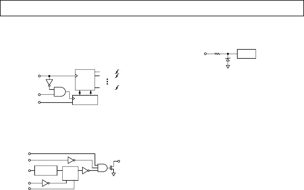
AD5203ARUZ100-REEL

AD5203
–9–REV. 0
OPERATION
The AD5203 provides a quad channel, 64-position digitally-
controlled variable resistor (VR) device. Changing the pro-
grammed VR settings is accomplished by clocking in an 8-bit
serial data word into the SDI (Serial Data Input) pin. The for-
mat of this data word is two address bits, MSB first, followed by
six data bits, MSB first. Table I provides the serial register data
word format. The AD5203 has the following address assign-
ments for the ADDR decode, which determines the location of
VR latch receiving the serial register data in Bits B5 through B0:
VR# = A1 × 2 + A0 + 1
VR outputs can be changed one at a time in random sequence.
The serial clock running at 10 MHz makes it possible to load all
four VRs in under 3.2 µs (8 × 4 × 100 ns) for the AD5203. The
exact timing requirements are shown in Figure 1.
The AD5203 resets to a midscale by asserting the RS pin, sim-
plifying initial conditions at power-up. Both parts have a power
shutdown SHDN pin that places the RDAC in a zero power
consumption state where terminals Ax are open-circuited and
the wiper Wx is connected to Bx, resulting in only leakage cur-
rents being consumed in the VR structure. In shutdown mode
the VR latch settings are maintained so that, returning to opera-
tional mode from power shutdown, the VR settings return to
their previous resistance values.
D5
D4
D3
D2
D1
D0
RDAC
LATCH
&
DECODER
Ax
Wx
Bx
R
S
= R
AB
/64
R
S
R
S
R
S
R
S
SHDN
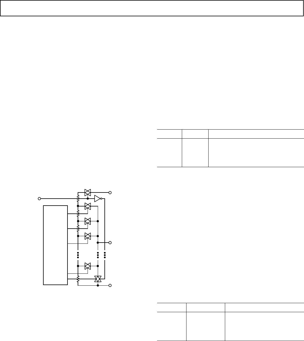
Figure 34. Equivalent RDAC Circuit
PROGRAMMING THE VARIABLE RESISTOR
Rheostat Operation
The nominal resistance of the RDAC between Terminals A and
B are available with values of 10 k, and 100 k. The final
digits of the part number determine the nominal resistance
value, e.g., 10 k = 10; 100 k = 100. The nominal resistance
(R
AB
) of the VR has 64 contact points accessed by the wiper
terminal, plus the B terminal contact. The 6-bit data word in
the RDAC latch is decoded to select one of the 64 possible
settings. The wiper’s first connection starts at the B terminal for
data 00
H
. This B–terminal connection has a wiper contact resis-
tance of 45 . The second connection (10 k part) is the first
tap point located at 201 [= R
BA
(nominal resistance)/64 + R
W
= 156 + 45 )] for data 01
H
. The third connection is the next
tap point representing 312 + 45 = 357 for data 02
H
. Each
LSB data value increase moves the wiper up the resistor ladder
until the last tap point is reached at 9889 . The wiper does not
directly connect to the B Terminal. See Figure 34 for a simpli-
fied diagram of the equivalent RDAC circuit.
The general transfer equation that determines the digitally pro-
grammed output resistance between Wx and Bx is:
R
WB
(Dx) = (Dx)/64 × R
BA
+ R
W
(1)
where Dx is the data contained in the 6-bit RDACx latch and
R
BA
is the nominal end-to-end resistance.
For example, when V
B
= 0 V and A–terminal is open circuit the
following output resistance values will be set for the following
RDAC latch codes (applies to the 10K potentiometer):
D (DEC) R
WB
() Output State
63 9889 Full-Scale
32 5045 Midscale (RS = 0 Condition)
1 201 1 LSB
0 45 Zero-Scale (Wiper Contact Resistance)
Note that in the zero-scale condition a finite wiper resistance of
45 is present. Care should be taken to limit the current flow
between W and B in this state to a maximum value of 5 mA to
avoid degradation or possible destruction of the internal switch
contact.
Like the mechanical potentiometer the RDAC replaces, it is
totally symmetrical. The resistance between the wiper W and
terminal A also produces a digitally controlled resistance R
WA
.
When these terminals are used the B–terminal should be tied to
the wiper. Setting the resistance value for R
WA
starts at a maxi-
mum value of resistance and decreases as the data loaded in the
latch is increased in value. The general transfer equation for this
operation is:
R
WA
(Dx) = (64-Dx)/64 × R
BA
+ R
W
(2)
where Dx is the data contained in the 6-bit RDACx latch and
R
BA
is the nominal end-to-end resistance. For example, when
V
A
= 0 V and B–terminal is tied to the wiper W, the following
output resistance values will be set for the following RDAC
latch codes:
D (DEC) R
WA
() Output State
63 201 Full-Scale
32 5045 Midscale (RS = 0 Condition)
1 9889 1 LSB
0 10045 Zero-Scale
The typical distribution of R
BA
from channel to channel matches
within ±1%. However, device-to-device matching is process-lot-
dependent, having a ±30% variation. The change in R
BA
with
temperature has a 700 ppm/°C temperature coefficient.
AD5203
–10– REV. 0
PROGRAMMING THE POTENTIOMETER DIVIDER
Voltage Output Operation
The digital potentiometer easily generates an output voltage
proportional to the input voltage applied to a given terminal.
For example connecting A–terminal to +5 V and B–terminal to
ground produces an output voltage at the wiper which can be
any value starting at zero volts up to 1 LSB less than +5 V.
Each LSB of voltage is equal to the voltage applied across ter-
minal AB divided by the 64 position resolution of the potenti-
ometer divider. The general equation defining the output
voltage with respect to ground for any given input voltage ap-
plied to terminals AB is:
V
W
(Dx) = Dx/64 × V
AB
+ V
B
Operation of the digital potentiometer in the divider mode
results in more accurate operation over temperature. Here the
output voltage is dependent on the ratio of the internal resistors
not the absolute value, therefore the drift improves to 20 ppm/°C.
DIGITAL INTERFACING
The AD5203 contains a standard three-wire serial input control
interface. The three inputs are clock (CLK), CS and serial data
input (SDI). The positive-edge sensitive CLK input requires
clean transitions to avoid clocking incorrect data into the serial
input register. Standard logic families work well. If mechanical
switches are used for product evaluation they should be de-
bounced by a flip-flop or other suitable means. The Figure 35
block diagram shows more detail of the internal digital cir-
cuitry. When CS is taken active low the clock loads data into
the serial register on each positive clock edge, see Table III.
AGND
A1
W1
B1
V
DD
AD5203
CS
CLK
6
D5
D0
EN
ADDR
DEC
A1
A0
SDI
DI
SER
REG
D0
D5
SDO
DO
DGND
A4
W4
B4
SHDN
RS
DAC
LAT
#1
R
R
D5
D0
DAC
LAT
#4
R
R
Figure 35. Block Diagram
The serial-data-output (SDO) pin contains an open drain
n-channel FET. This output requires a pull-up resistor in order
to transfer data to the next package’s SDI pin. The pull-up
resistor termination voltage may be larger than the V
DD
supply
of the AD5203 SDO output device, e.g., the AD5203 could
operate at V
DD
= 3.3 V and the pull-up for interface to the next
device could be set at +5 V. This allows for daisy chaining sev-
eral RDACs from a single processor serial data line. Clock pe-
riod needs to be increased when using a pull-up resistor to the
SDI pin of the following device in the series. Capacitive loading
at the daisy chain node SDO-SDI between devices must be
accounted for to successfully transfer data. When daisy chaining
is used, the CS should be kept low until all the bits of every
package are clocked into their respective serial registers insuring
that the address bits and data bits are in the proper decoding
location. This would require 16 bits of address and data comply-
ing to the word format provided in Table I if two AD5203 four-
channel RDACs are daisy chained. During shutdown, SHDN
the SDO output pin is forced to the off (logic high state) to
disable power dissipation in the pull-up resistor. See Figure 37
for equivalent SDO output circuit schematic.
Table II. Input Logic Control Truth Table
CLK CS RS SHDN Register Activity
L L H H No SR effect, enables SDO pin.
P L H H Shift one bit in from the SDI pin.
The eighth previously entered bit
is shifted out of the SDO pin.
X P H H Load SR data into RDAC latch
based on A1, A0 decode (Table III).
X H H H No Operation.
X X L H Sets all RDAC latches to midscale,
wiper centered and SDO latch
cleared.
X H P H Latches all RDAC latches to 20
H
.
X H H L Open circuits all Resistor A–termi-
nals, connects W to B, turns off
SDO output transistor.
NOTE: P = positive edge, X = don’t care, SR = shift register.
Table III. Address Decode Table
A1 A0 Latch Decoded
0 0 RDAC#1
0 1 RDAC#2
1 0 RDAC#3
1 1 RDAC#4
AD5203
–11–REV. 0
The data setup and data hold times in the specification table
determine the data valid time requirements. The last eight bits
of the data word entered into the serial register are held when
CS returns high. At the same time CS goes high it gates the
address decoder which enables one of four positive edge trig-
gered RDAC latches, see Figure 36 detail.
RDAC 1
RDAC 2
RDAC 4
AD5203
SDI
CLK
CS
ADDR
DECODE
SERIAL
REGISTER
Figure 36. Equivalent Input Control Logic
The target RDAC latch is loaded with the last six bits of the
serial data word completing one RDAC update. Four separate
8-bit data words must be clocked in to change all four VR
settings.
SERIAL
REGISTER
SDI
CK
RS
D
Q
SHDN
CS
CLK
RS
SDO
Figure 37. Detail, SDO Output Schematic of the AD5203
All digital inputs are protected with a series input resistor and
parallel Zener ESD structure shown in Figure 38. Applies to
digital input pins CS, SDI, SDO, RS, SHDN, CLK.
1kV
LOGIC
Figure 38. Equivalent ESD Protection Circuit
DYNAMIC CHARACTERISTICS
The total harmonic distortion plus noise (THD+N) measures
0.003% using an offset ground with a rail-to-rail OP279 invert-
ing op amp test circuit, see Figure 30. Figure 15 plots THD
versus frequency for both inverting and noninverting amplifier
topologies. Thermal noise is primarily Johnson noise, typically
9 nV/Hz for the 10 k version measured at 1 kHz. For the
100 k device, thermal noise measures 29 nV/Hz. Channel-to-
channel crosstalk measures less than –65 dB at f = 100 kHz. To
achieve this isolation, the extra ground pins (AGND) located
between the potentiometer terminals (A, B, W) must be con-
nected to circuit ground. The AGND and DGND pins should
be at the same voltage potential. Any unused potentiometers in
a package should be connected to ground. Power supply rejec-
tion is typically –50 dB at 10 kHz (care is needed to minimize
power supply ripple injection in high accuracy applications).

AD5203ARUZ100-REEL

Mfr. #:
Manufacturer:
Analog Devices Inc.
Description:
Digital Potentiometer ICs IC QUAD 6-BIT
Lifecycle:
New from this manufacturer.
Delivery:
DHL FedEx Ups TNT EMS
Payment:
T/T Paypal Visa MoneyGram Western Union