1
LTC1433/LTC1434
450mA, Low Noise
Current Mode Step-Down
DC/DC Converters
Cellular Telephones
Portable Instruments
Wireless Modems
RF Communications
Distributed Power Systems
Scanners
Battery-Powered Equipment
DESCRIPTION
U
High Efficiency: Up to 93%
Constant Frequency Adaptive Power
TM
Operation
Input Voltage Range: 3V to 13.5V
Internal 0.6 Power Switch (V
IN
= 10V)
Low Dropout Operation: 100% Duty Cycle
Low-Battery Detector
Internal Power-On Reset Timer
Current Mode Operation for Excellent Line and Load
Transient Response
Low Quiescent Current: 470µA
Shutdown Mode Draws Only 15µA Supply Current
±1% Reference Accuracy
Available in 16- and 20-Lead Narrow SSOP
FEATURES
The LTC
®
1433/LTC1434 are monolithic pulse width modu-
lated step-down DC/DC converters. By utilizing current
mode switching techniques, they provide excellent AC and
DC load and line regulation. Both devices operate at a fixed
frequency with the LTC1434 phase-lockable to an external
clock signal.
Both devices incorporate two internal P-channel power
MOSFETs with a parallel combined resistance of 0.6 (at
a supply of 10V). The Adaptive Power output stage selec-
tively drives one or both of the switches at frequencies up
to 700kHz to reduce switching losses and maintain high
efficiencies at low output currents.
The LTC1433/LTC1434 are capable of supplying up to
450mA of output current and boasts a ±2.4% output
voltage accuracy. An internal low-battery detector has the
same level of accuracy as the output voltage. A power-on
reset timer (POR) is included which generates a signal
delayed by 65536/f
CLK
(300ms typ) after the output is
within 5% of the regulated output voltage.
Ideal for current sensitive applications, the devices draw
only 470µA of quiescent current. In shutdown the devices
draw a mere 15µA. To further maximize the life of the
battery source, the internal P-channel MOSFET switch is
turned on continuously in dropout.
APPLICATIONS
U
, LTC and LT are registered trademarks of Linear Technology Corporation.
Adaptive Power is a trademark of Linear Technology Corporation.
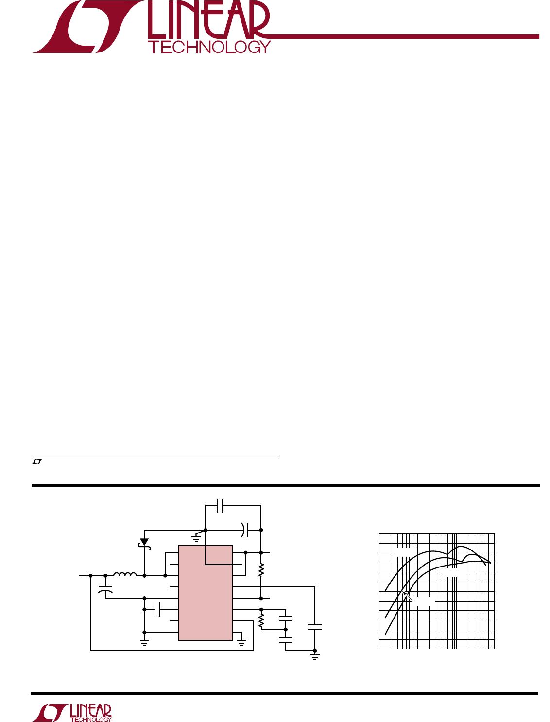
TYPICAL APPLICATION
U
1
2
3
4
5
6
7
8
16
15
14
13
12
11
10
9
SSW
NC
BSW
NC
SGND
RUN/SS
LBO
LBI
PWRV
IN
SV
IN
C
OSC
POR
I
TH
V
OSENSE
V
PROG
LTC1433
PGND
68µF**
20V
0.1µF
0.1µF
100µF*
10V
D1:MOTOROLA MBRS130LT3
L1: COILCRAFT D03316-104
V
OUT
3.3V
D1
L1
100µH
POWER-ON
RESET
V
IN
3.5V TO 12V
680pF
5.1k
10k
6800pF
47pF
1433/34 F01
* AVX TPSD107M010R0100
** AVX TPSE686M020R0150
+
+
Figure 1. High Efficiency Step-Down Converter
LOAD CURRENT (A)
0.001
60
EFFICIENCY (%)
70
80
0.01 0.1 1
1433/34 TA01
50
40
100
90
V
IN
= 5V
V
IN
= 12V
V
IN
= 9V
LTC1433 Efficiency for
V
OUT
= 3.3V
2
LTC1433/LTC1434
A
U
G
W
A
W
U
W
ARB
S
O
LU
T
EXI T
I
S
(Voltages Referred to PGND Pin)
Input Supply Voltage (PWRV
IN
, SV
IN
) ... 13.5V to –0.3V
DC Small Switch Current (SSW)......................... 100mA
Peak Small Switch Current (SSW) ..................... 300mA
Small Switch Voltage
(SSW)................................(V
IN
+ 0.3V) to (V
IN
– 13.5V)
DC Large Switch Current (BSW)....................... 600mA
Peak Large Switch Current (BSW) .......................... 1.2A
Large Switch Voltage
(BSW)................................(V
IN
+ 0.3V) to (V
IN
– 13.5V)
PLLIN, PLL LPF, I
TH
, C
OSC
........................2.7V to –0.3V
POR, LBO ..................................................12V to –0.3V
LBI, V
OSENSE
..............................................10V to –0.3V
RUN/SS, V
PROG
Voltages
V
IN
11.7V ...........................................12V to –0.3V
V
IN
< 11.7V...............................(V
IN
+ 0.3V) to –0.3V
Commercial Temperature Range
LTC1433C/LTC1434C .............................. 0°C to 70°C
Extended Commercial Operating Temperature
Range (Note 2) ....................................... 40°C to 85°C
Industrial Temperature Range (Note 3)
LTC1433I/LTC1434I ........................... 40°C to 85°C
Junction Temperature (Note 4)............................. 125°C
Storage Temperature Range ................. 65°C to 150°C
Lead Temperature (Soldering, 10 sec).................. 300°C
(Note 1)
WU
U
PACKAGE
/
O
RDER I FOR ATIO
ORDER PART
NUMBER
ORDER PART
NUMBER
LTC1433CGN
LTC1433IGN
LTC1434CGN
LTC1434IGN
T
JMAX
= 125°C, θ
JA
= 150°C/W
T
JMAX
= 125°C, θ
JA
= 150°C/W
1
2
3
4
5
6
7
8
TOP VIEW
GN PACKAGE
16-LEAD PLASTIC SSOP
16
15
14
13
12
11
10
9
SSW
NC
BSW
NC
SGND
RUN/SS
LBO
LBI
PWRV
IN
PGND
SV
IN
C
OSC
POR
I
TH
V
OSENSE
V
PROG
Consult factory for Military grade parts.
1
2
3
4
5
6
7
8
9
10
TOP VIEW
GN PACKAGE
20-LEAD PLASTIC SSOP
20
19
18
17
16
15
14
13
12
11
NC
SSW
NC
BSW
SGND
NC
RUN/SS
NC
LBO
LBI
PWRV
IN
PGND
SV
IN
PLLIN
PLL LPF
C
OSC
POR
I
TH
V
OSENSE
V
PROG
ELECTRICAL CHARACTERISTICS
T
A
= 25°C, V
IN
= 10V, V
RUN/SS
= 5V, unless otherwise noted. (Notes 2, 3)
SYMBOL PARAMETER CONDITIONS MIN TYP MAX UNITS
Main Control Loop
I
IN
V
OSENSE
Feedback Current V
PROG
Pin Open (Note 5) 10 50 nA
V
OSENSE
Regulated Output Voltage (Note 5)
1.19V (Adjustable) Selected V
PROG
Pin Open 1.178 1.190 1.202 V
3.3V Selected V
PROG
= 0V 3.220 3.300 3.380 V
5V Selected V
PROG
= V
IN
4.880 5.000 5.120 V
V
OVL
Output Overvoltage Lockout V
PROG
Pin Open 1.24 1.28 1.32 V
V
OSENSE
Reference Voltage Line Regulation V
IN
= 3.6V to 13V (Note 5), V
PROG
Pin Open 0.002 0.01 %/V
V
LOADREG
Output Voltage Load Regulation I
TH
Sinking 5µA (Note 5) 0.5 0.8 %
I
TH
Sourcing 5µA (Note 5) 0.5 0.8 %
3
LTC1433/LTC1434
ELECTRICAL CHARACTERISTICS
T
A
= 25°C, V
IN
= 10V, V
RUN/SS
= 5V, unless otherwise noted.
The denotes specifications which apply over the specified temperature
range.
Note 1: Absolute Maximum Ratings are those values beyond which the life
of a device may be impaired.
Note 2: C-grade device specifications are guaranteed over the 0°C to 70°C
temperature range. In addition, C-grade device specifications are assured
over the – 40°C to 85°C temperature range by design or correlation, but
are not production tested.
Note 3: I-grade device specifications are guaranteed over the – 40°C to
85°C temperature range by design, testing or correlation.
Note 4: T
J
is calculated from the ambient temperature T
A
and power
dissipation P
D
according to the following formula:
LTC1433/LTC1434: T
J
= T
A
+ (P
D
)(150°C/W)
Note 5: The LTC1433/LTC1434 are tested in a feedback loop which servos
V
OSENSE
to the feedback point for the error amplifier (V
ITH
= 1.19V).
Note 6: Dynamic supply current is higher due to the gate charge being
delivered at the switching frequency.
Note 7: Oscillator frequency is tested by measuring the C
OSC
charge and
discharge currents and applying the formula:
f
OSC
(kHz) =
+
–1
8.4(10
8
)
C
OSC
(pF) + 11
()
1
I
CHG
()
1
I
DIS
SYMBOL PARAMETER CONDITIONS MIN TYP MAX UNITS
I
PROG
V
PROG
Input Current 0.5V > V
PROG
–4 –10 µA
V
IN
– 0.5V < V
PROG
< V
IN
4 10 µA
Main Control Loop
I
Q
Input DC Supply Current (Note 6)
Normal Mode 3.6V < V
IN
< 13V 470 µA
Shutdown, Reference Alive V
RUN/SS
= 0V, 3.6V < V
IN
< 13V, LBI > 0.9V 35 70 µA
Complete Shutdown V
RUN/SS
= 0V, 3.6V < V
IN
< 13V, LBI 0.48V 15 30 µA
V
RUN/SS
RUN/SS Threshold 0.8 1.3 2 V
I
RUN/SS
Soft Start Current Source V
RUN/SS
= 0V 1.2 3 4.5 µA
Oscillator and Phase-Locked Loop
f
OSC
Oscillator Frequency C
OSC
= 100pF (Note 7) 112 125 142 kHz
V
CO
High V
PLL LPF
= 2.4V 200 240 kHz
R
PLLIN
PLL Input Resistance 50 k
I
PLL LPF
Phase Detector Output Current
Sinking Capability f
PLLIN
< f
OSC
10 15 20 µA
Sourcing Capability f
PLLIN
> f
OSC
10 15 20 µA
Power-On Reset
V
SATPOR
POR Saturation Voltage I
POR
= 1.6mA, V
OSENSE
= 1V, V
PROG
Open 0.6 1.0 V
I
LPOR
POR Leakage V
POR
= 10V, V
OSENSE
= 1.2V, V
PROG
Open 0.2 1.0 µA
V
TRPOR
POR Trip Voltage from Regulated V
PROG
Pin Open, V
OSENSE
Ramping Negative 11 7.5 4 %
Output
t
DPOR
POR Delay V
PROG
Pin Open 65536 Cycles
Low-Battery Comparator
V
SATLBO
LBO Saturation Voltage I
LBO
= 1.6mA, V
LBI
= 1.1V 0.6 1.0 V
I
LLBO
LBO Leakage V
LBO
= 10V, V
LBI
= 1.4V 0.01 1.0 µA
V
TRLBI
LBI Trip Voltage High to Low Transition on LBO 1.16 1.19 1.22 V
V
HYSTLB
Low-Battery Comparator Hysteresis 40 mV
V
SDLB
Low-Battery Shutdown Trip Point 0.74 V
I
INLBI
LBI Input Current V
LBI
= 1.19V 1 50 nA
P-Channel Power FETs Characteristics
R
SMFET
R
DS(ON)
of Small FET I
SSW
= 15mA 3.3 4.1
R
BIGFET
R
DS(ON)
of Big FET I
BSW
= 150mA 0.8 1.2
I
LSSW
Small FET Leakage V
RUN/SS
= 0V 7 1000 nA
I
LBSW
Big FET Leakage V
RUN/SS
= 0V 5 1000 nA

LTC1434IGN#TRPBF

Mfr. #:
Manufacturer:
Analog Devices / Linear Technology
Description:
Switching Voltage Regulators 450mA, L N C Mode Buck DC/DC Conv
Lifecycle:
New from this manufacturer.
Delivery:
DHL FedEx Ups TNT EMS
Payment:
T/T Paypal Visa MoneyGram Western Union