10
LTC1433/LTC1434
APPLICATIONS INFORMATION
WUU
U
Efficiency Considerations
Since there are two separate pins for the drain of the small
and large P-channel switch, we could utilize two induc-
tors to further enhance the efficiency of the regulator over
the low load current range. Figure 4 shows the circuit
connection.(Also refer to the Typical Applications sec-
tion.)
Figure 4. Using Two Inductors for Higher Low Current Efficiency
BSW
SSW
D1
D2
1433/34 F04
L2
L1
LTC1433/
LTC1434
To reduce core losses, the user can use a higher value
inductor on the small P-channel switch. Since this switch
only carries a small part of the overall current, the user can
still use a small physical size inductor without sacrificing
on copper losses. The Schottky diode can also be chosen
with a lower current rating. For the graph in Figure 5, a
Coilcraft DT1608C series inductor is used along with a
MBRS0520LT3 Schottky diode on the SSW pin. As can be
seen from Figure 5, the average efficiency gain over the
region where the small P-channel is on is about 3%.
LOAD CURRENT (A)
0.001
60
EFFICIENCY (%)
70
80
0.01 0.1 1
1433/34 • F05
50
40
100
90
V
IN
= 5V
V
IN
= 9V
ONE 22µH INDUCTOR
ON SSW AND BSW
100µH ON SSW
22µH ON BSW
V
OUT
= 3.3V
C
OSC
= 47pF
Figure 5. Efficiency Comparison Between Single Inductor
and Dual Inductor
Hence, the dual inductor configuration is good for the user
who requires as high an efficiency as possible at low load
while retaining constant frequency operation.
Output Voltage Programming
The LTC1433/LTC1434 family all have pin selectable out-
put voltage programming. The output voltage is selected
by the V
PROG
pin as follows:
V
PROG
= 0V V
OUT
= 3.3V
V
PROG =
V
IN
V
OUT
= 5V
V
PROG
= Open (DC) V
OUT
= Adjustable
The LTC1433/LTC1434 family also has remote output
voltage sense capability. The top of the internal resistive
divider is internally connected to V
OSENSE
. For fixed output
voltage applications, the V
OSENSE
pin is connected to the
output voltage as shown in Figure 6. When using an
external resistive divider, the V
PROG
pin is left open DC and
the V
OSENSE
pin is connected to the feedback resistors as
shown in Figure 7. To prevent stray pickup, a 100pF
capacitor is suggested across R1 located close to the
LTC1433/LTC1434.
R1
R2
OPEN (DC)
1433/34 F07
100pF
V
OUT
V
PROG
SGND
LTC1433/
LTC1434
V
OSENSE
V
OUT
= 1.19V 1 +
R2
R1
()
Figure 7. LTC1433/LTC1434 Adjustable Applications
V
PROG
SGND
LTC1433/
LTC1434
1433/34 F06
C
OUT
V
OUT
GND: V
OUT
= 3.3V
V
IN
: V
OUT
= 5V
+
V
OSENSE
Figure 6. LTC1433/LTC1434 Fixed Output Applications
11
LTC1433/LTC1434
APPLICATIONS INFORMATION
WUU
U
Power-On Reset Function (POR)
The power-on reset function monitors the output voltage
and turns on an open-drain device when it is out of
regulation. An external pull-up resistor is required on the
POR pin.
When power is first applied or when coming out of
shutdown, the POR output is pulled to ground. When the
output voltage rises above a level which is 5% below the
regulated output value, an internal counter starts. After
counting 2
16
(65536) clock cycles the POR pull-down
device turns off.
The POR output will go low whenever the output voltage
drops below 7.5% of its regulated value for longer than
approximately 30µs, signaling an out-of-regulation condi-
tion. In shutdown the POR output is pulled low even if the
regulator’s output is held up by an external source.
Run/Soft Start Function
The RUN/SS pin is a dual purpose pin which provides the
soft start function and a means to shut down the LTC1433/
LTC1434. Soft start reduces input surge currents by
providing a gradual ramp-up of the internal current limit.
Power supply sequencing can also be accomplished using
this pin.
An internal 3µA current source charges up an external
capacitor C
SS.
When the voltage on RUN/SS reaches 1.3V
the LTC1433/LTC1434 begins operating. As the voltage
on RUN/SS continues to ramp from 1.3V to 2.4V the
internal current limit is also ramped at a proportional
linear rate. The current limit begins at approximately
350mA (at V
RUN/
SS
= 1.3V) and ends at 1.2A (V
RUN/SS
=
2.4V). The output voltage thus ramps up slowly, charging
the output capacitor while input surge currents are re-
duced. If RUN/SS has been pulled all the way to ground
there is a delay of approximately 0.5s/µF before starting,
followed by a like time to reach full current.
t
DELAY
= 5(10
5
)C
SS
seconds
By pulling the RUN/SS pin below 1.3V, the LTC1433/
LTC1434 are put in low current shutdown. This pin can be
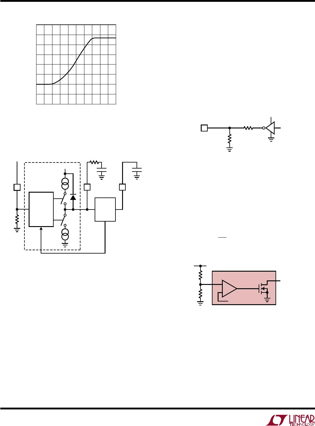
driven directly from logic as shown in Figure 8. Diode D1
in Figure 8 reduces the start delay but allows C
SS
to ramp
up slowly providing the soft start function. This diode can
be deleted if soft start is not needed. The RUN/SS pin has
an internal 6V Zener clamping the voltage on this pin (see
Functional Diagram).
1433/34 F08
C
SS
D1
RUN/SS
C
SS
RUN/SS
Figure 8. RUN/SS Pin Interfacing
Phase-Locked Loop and Frequency Synchronization
The LTC1434 has an internal voltage-controlled oscilla-
tor and phase detector comprising a phase-locked loop.
This allows the MOSFET turn-on to be locked to the rising
edge of an external source. The frequency range of the
voltage-controlled oscillator is ±30% around the center
frequency f
O
. The value of C
OSC
is calculated from the
desired operating frequency (f
O
) with the following
expression (assuming the phase-locked loop is locked,
i.e V
PLL LPF
= 1.19V):
C
Frequency
OSC
pF
kHz
()
=
()
206 10
11
4
.
Instead of using the above expression, Figure 2 graphi-
cally shows the relationship between the oscillator fre-
quency and the value of C
OSC
under various voltage
conditions at the PLL LPF pin.
The phase detector used is an edge sensitive digital type
which provides zero degrees phase shift between the
external and internal oscillators. This type of phase detector
will not lock up on input frequencies close to the harmonics
of the V
CO
center frequency. The PLL hold-in range f
H
is
equal to the capture range, f
H
= f
C
= ±0.3f
O.
The output of the phase detector is a pair of complemen-
tary current sources charging or discharging the external
filter network on the PLL LPF pin. The relationship
between the voltage on the PLL LPF pin and operating
frequency is shown in Figure 9. A simplified block diagram
is shown in Figure 10.
12
LTC1433/LTC1434
APPLICATIONS INFORMATION
WUU
U
Figure 10. Phase-Locked Loop Block Diagram
PLLIN
50k
1433/34 F10
PLL LPF C
OSC
PHASE
DETECTOR
OSC
R
LP
C
LP
C
OSC
EXTERNAL
FREQUENCY
2.4V
DIGITAL
PHASE/
FREQUENCY
DETECTOR
V
PLLLPF
(V)
0
FREQUENCY (kHz)
1.3f
O
0.7f
O
1433/34 F09
1.5 2.01.00.5
2.5
f
O
Figure 9. Relationship Between Oscillator Frequency
and Voltage at PLL LPF Pin
If the external frequency (V
PLLIN
) is greater than the center
frequency f
0
, current is sourced continuously, pulling up
the PLL LPF pin. When the external frequency is less than
f
0
, current is sunk continuously, pulling down the PLL LPF
pin. If the external and internal frequencies are the same
but exhibit a phase difference, the current sources turn on
for an amount of time corresponding to the phase differ-
ence. Thus the voltage on the PLL LPF pin is adjusted until
the phase and frequency of the external and internal
oscillators are identical. At this stable operating point the
phase comparator output is open and the filter capacitor
C
LP
holds the voltage.
The loop filter components C
LP
and R
LP
smooth out the
current pulses from the phase detector and provide a
stable input to the voltage controlled oscillator. The filter
components C
LP
and R
LP
determine how fast the loop
acquires lock. Typically R
LP
= 10k and C
LP
is 0.01µF to
0.1µF. Be sure to connect the low side of the filter to SGND.
The PLL LPF pin can be driven with external logic to obtain
a 1:1.9 frequency shift. The circuit shown in Figure 11 will
provide a frequency shift from f
O
to 1.9f
O
as the voltage
V
PLL LPF
increases from 0V to 2.4V.
Do not exceed 2.4V on
V
PLL LPF
.
Figure 11. Directly Driving PLL LPF Pin
PLL LPF
2.4V MAX
3.3V OR 5V
1433/34 F11
18k
Low-Battery Comparator
The LTC1433/LTC1434 have an on-chip, low-battery com-
parator which can be used to sense a low-battery condi-
tion when implemented as shown in Figure 12. The resis-
tor divider R3/R4 sets the comparator trip point as follows:
V
R
R
LBTRIP
=+
119
4
3
1.
+
V
IN
R4
R3
1433/34 F12
1.19V REFERENCE
LTC1433/LTC1434
Figure 12. Low-Battery Comparator
The divided down voltage at the negative (–) input to the
comparator is compared to an internal 1.19V reference. A
40mV hysteresis is built in to assure rapid switching. The
output is an open-drain MOSFET and requires a pull-up
resistor to operate. This comparator is active in shutdown.
To save more shutdown quiescent current, this compara-
tor can be shut down by taking the LBI pin below 0.74V,

LTC1434IGN#TRPBF

Mfr. #:
Manufacturer:
Analog Devices / Linear Technology
Description:
Switching Voltage Regulators 450mA, L N C Mode Buck DC/DC Conv
Lifecycle:
New from this manufacturer.
Delivery:
DHL FedEx Ups TNT EMS
Payment:
T/T Paypal Visa MoneyGram Western Union