13
LTC2846
sn2846 2846fs
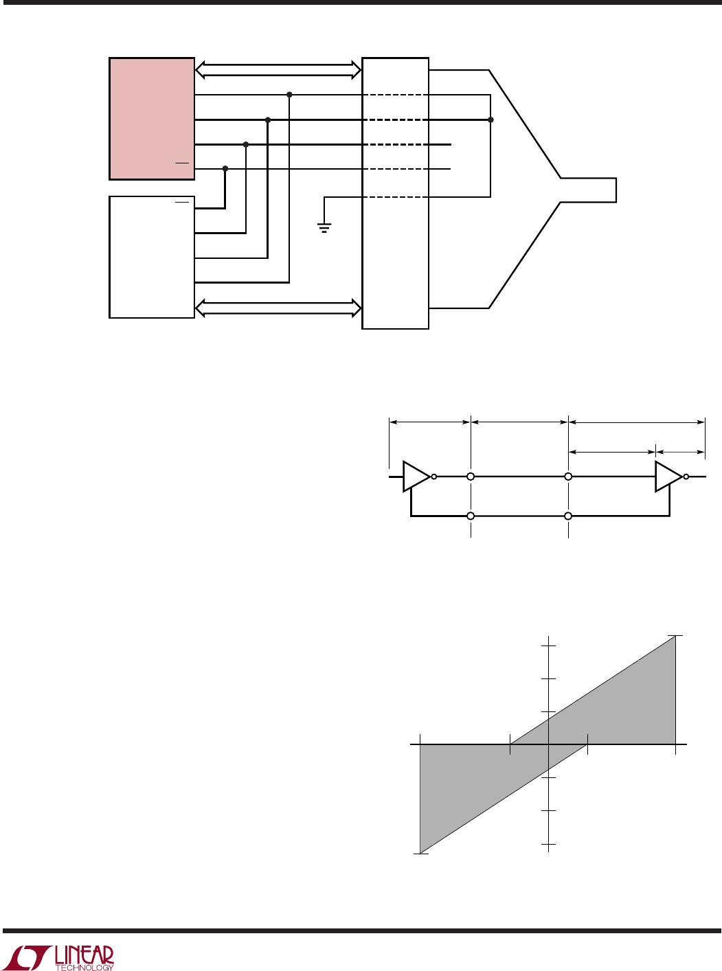
Figure 18. Single Port DCE V.35 Mode Selection in the Cable
Figure 20. V.10 Receiver Input Impedance
Figure 19. Typical V.10 Interface
APPLICATIO S I FOR ATIO
WUUU
selected. Switching the terminations with FETs is difficult
because the FETs must remain off when the signal voltage
is beyond the supply voltage. Alternatively, custom cables
may contain termination in the cable head or route signals
to various terminations on the board.
The LTC2846/LTC2844 chip set solves the cable termina-
tion switching problem by automatically providing the
appropriate termination and switching on-chip for the
V.10 (RS423), V.11 (RS422), V.28 (RS232) and V.35
electrical protocols.
V.10 (RS423) Interface
All V.10 drivers and receivers necessary for the RS449,
EIA530, EIA530-A, V.36 and X.21 protocols are imple-
mented on the LTC2844 or LTC2845.
A typical V.10 unbalanced interface is shown in Figure 19.
A V.10 single-ended generator with output A and ground
C is connected to a differential receiver with input A' con-
nected to A, and ground C' connected via the signal return
to ground C. Usually, no cable termination is required for
V.10 interfaces, but the receiver inputs must be compliant
with the impedance curve shown in Figure 20.
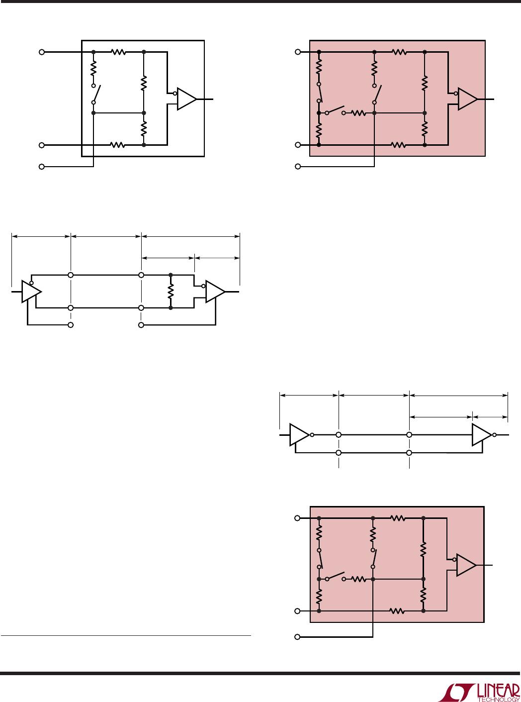
The V.10 receiver configuration in the LTC2844 and
LTC2845 is shown in Figure 21. In V.10 mode, switch S3
inside the LTC2844 and LTC2845 is turned off. The
noninverting input is disconnected inside the LTC2844
NC
NC
CABLE
2846 F18
15
16
18
19
LTC2846
LTC2844
CONNECTOR
14
13
12
11
(DATA)
M0
M1
M2
DCE/DTE
DCE/DTE
M2
M1
M0
(DATA)
AA
'
CC
'
GENERATOR
BALANCED
INTERCONNECTING
CABLE
LOAD
CABLE
TERMINATION
RECEIVER
2846 F19
I
Z
V
Z
10V
–3.25mA
3.25mA
–3V
3V 10V
2846 F20
14
LTC2846
sn2846 2846fs
Figure 22. Typical V.11 Interface
Figure 21. V.10 Receiver Configuration
Figure 24. Typical V.28 Interface
Figure 25. V.28 Receiver Configuration
Figure 23. V.11 Receiver Configuration
1
Actually, there is no switch S1 in receivers R2 and R3. However, for simplicity, all termination
networks on the LTC2846 can be treated identically if it is assumed that an S1 switch exists and is
always closed on the R2 and R3 receivers.
APPLICATIO S I FOR ATIO
WUUU
and LTC2845 receivers and connected to ground. The
cable termination is then the 30k input impedance to
ground of the LTC2844 and LTC2845 V.10 receiver.
V.11 (RS422) Interface
A typical V.11 balanced interface is shown in Figure 22. A
V.11 differential generator with outputs A and B and
ground C is connected to a differential receiver with input
A' connected to A, input B' connected to B, and ground C'
connected via the signal return to ground C. The V.11
interface has a differential termination at the receiver end
that has a minimum value of 100. The termination
resistor is optional in the V.11 specification, but for the
high speed clock and data lines, the termination is essen-
tial to prevent reflections from corrupting the data. The
receiver inputs must also be compliant with the imped-
ance curve shown in Figure 20.
In V.11 mode, all switches are off except S1 of the
LTC2846’s receivers which connects a 103 differential
termination impedance to the cable as shown in Figure
23
1
. The LTC2844 and LTC2845 only handle control
signals, so no termination other than their V.11 receivers’
30k input impedance is necessary.
V.28 (RS232) Interface
A typical V.28 unbalanced interface is shown in Figure 24.
A V.28 single-ended generator with output A and ground
C is connected to a single-ended receiver with input A'
connected to A and ground C' connected via the signal
return to ground C.
R5
20k
LTC2844
RECEIVER
2846 F21
A
B
A
'
B'
C'
R8
6k
S3
R6
10k
R7
10k
GND
R4
20k
AA'
B
C
B'
C'
GENERATOR
BALANCED
INTERCONNECTING
CABLE
LOAD
CABLE
TERMINATION
RECEIVER
100
MIN
2846 F22
R3
124
R5
20k
LTC2846
RECEIVER
2846 F23
A
'
B
'
C
'
R1
51.5
R8
6k
S2
S3
R2
51.5
R6
10k
R7
10k
GND
R4
20k
S1
AA
'
CC
'
GENERATOR
BALANCED
INTERCONNECTING
CABLE
LOAD
CABLE
TERMINATION
RECEIVER
2846 F24
R3
124
R5
20k
LTC2846
RECEIVER
2846 F25
A
'
B
'
C
'
R1
51.5
R8
6k
S2
S3
R2
51.5
R6
10k
R7
10k
GND
R4
20k
S1
15
LTC2846
sn2846 2846fs
Figure 28. Charge Pump
Figure 27. V.35 Receiver Configuration
Figure 26. Typical V.35 Interface
APPLICATIO S I FOR ATIO
WUUU
In V.28 mode, S3 is closed inside the LTC2846/LTC2844
which connects a 6k (R8) impedance to ground in parallel
with 20k (R5) plus 10k (R6) for a combined impedance of
5k as shown in Figure 25. Proper termination is only pro-
vided when the B input of the receivers is floating, since S1
of the LTC2846’s R2 and R3 receivers remains on in V.28
mode
1
. The noninverting input is disconnected inside the
LTC2846/LTC2844 receiver and connected to a TTL level
reference voltage to give a 1.4V receiver trip point.
V.35 Interface
A typical V.35 balanced interface is shown in Figure 26. A
V.35 differential generator with outputs A and B and
ground C is connected to a differential receiver with input
A' connected to A, input B' connected to B, and ground C'
connected via the signal return to ground C. The V.35
interface requires a T or delta network termination at the
receiver end and the generator end. The receiver differen-
tial impedance measured at the connector must be
A
A
'
B
C
B
'
C
'
GENERATOR
BALANCED
INTERCONNECTING
CABLE
LOAD
CABLE
TERMINATION
RECEIVER
2846 F26
50
125
50
50
125
50
R3
124
R5
20k
LTC2846
RECEIVER
2846 F27
A
'
B
'
C
'
R1
51.5
R8
6k
S2
S3
R2
51.5
R6
10k
R7
10k
GND
R4
20k
S1
100±10, and the impedance between shorted termi-
nals (A' and B') and ground (C') must be 150 ±15.
In V.35 mode, both switches S1 and S2 inside the LTC2846
are on, connecting a T network impedance as shown in
Figure 27. The 30k input impedance of the receiver is
placed in parallel with the T network termination, but does
not affect the overall input impedance significantly.
The generator differential impedance must be 50 to
150 and the impedance between shorted terminals (A
and B) and ground (C) must be 150 ±15.
No-Cable Mode
The no-cable mode (M0 = M1 = M2 = 1) is intended for
the case when the cable is disconnected from the con-
nector. The charge pump, bias circuitry, drivers and
receivers are turned off, the driver outputs are forced into
a high impedance state, and the
V
CC
supply current to the
transceiver drops to less than 300µA while its
V
IN
supply
current drops to less than 10µA. Note that the LTC2846’s
R2 and R3 receivers continue to be terminated by a 103
differential impedance.
Charge Pump
The LTC2846 uses an internal capacitive charge pump to
generate V
DD
and V
EE
as shown in Figure 28. A voltage
doubler generates about 8V on V
DD
and a voltage inverter
generates about – 7.5V on V
EE
. Three 1µF surface mounted
tantalum or ceramic capacitors are required for C1, C2 and
C3. The V
EE
capacitor C4 should be a minimum of 3.3µF.
All capacitors are 16V and should be placed as close as
possible to the LTC2846 to reduce EMI.
33
32
31
30
2846 F28
7
6
5
8
C3
1µF
C5
10µF
5V
C1
1µF
C2
1µF
C4
3.3µF
LTC2846
V
DD
C1
+
C1
V
CC
C2
+
C2
V
EE
GND
+

LTC2846IG#TRPBF

Mfr. #:
Manufacturer:
Analog Devices Inc.
Description:
RS-232 Interface IC 3.3V Multiprotocol CLK_DATA Xcvr
Lifecycle:
New from this manufacturer.
Delivery:
DHL FedEx Ups TNT EMS
Payment:
T/T Paypal Visa MoneyGram Western Union