4
LTC2846
sn2846 2846fs
The denotes specifications which apply over the full operating
temperature range, otherwise specifications are at T
A
= 25°C. V
CC
= 5V, V
IN
= 3.3V, V
SHDN
= V
IN
, unless otherwise noted. (Notes 2, 3)
ELECTRICAL CHARACTERISTICS
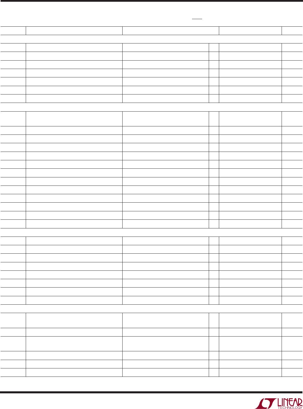
SYMBOL PARAMETER CONDITIONS MIN TYP MAX UNITS
V.11 Receiver
V
TH
Input Threshold Voltage 7V V
CM
7V 0.2 0.2 V
V
TH
Input Hysteresis 7V V
CM
7V 15 40 mV
R
IN
Input Impedance 7V V
CM
7V (Figure 3) 100 103
t
r
, t
f
Rise or Fall Time C
L
= 50pF (Figures 4, 14) 15 ns
t
PLH
Input to Output Rising C
L
= 50pF (Figures 4, 14) 50 90 ns
t
PHL
Input to Output Falling C
L
= 50pF (Figures 4, 14) 50 90 ns
t Input to Output Difference, t
PLH
– t
PHL
C
L
= 50pF (Figures 4, 14) 0425 ns
V.35 Driver
V
OD
Differential Output Voltage Open Circuit, R
L
= 1.95k (Figure 5) ±1.2 V
With Load, –4V V
CM
4V (Figure 6) ±0.44 ±0.55 ±0.66 V
V
OA
, V
OB
Single-Ended Output Voltage Open Circuit, R
L
= 1.95k (Figure 5) ±1.2 V
V
OC
Transmitter Output Offset R
L
= 50 (Figure 5) ±0.6 V
I
OH
Transmitter Output High Current V
A
,
V
B
= 0V –9 11 –13 mA
I
OL
Transmitter Output Low Current V
A
,
V
B
= 0V 91113 mA
I
OZ
Transmitter Output Leakage Current V
A
and V
B
0.25V ±1 ±100 µA
R
OD
Transmitter Differential Mode Impedance 50 100 150
R
OC
Transmitter Common Mode Impedance 2V V
CM
2V (Figure 7) 135 150 165
t
r
, t
f
Rise or Fall Time (Figures 8, 13) 5 ns
t
PLH
Input to Output (Figures 8, 13) 15 35 65 ns
t
PHL
Input to Output (Figures 8, 13) 15 35 65 ns
t Input to Output Difference, t
PLH
– t
PHL
(Figures 8, 13) 016 ns
t
SKEW
Output to Output Skew (Figures 8, 13) 4 ns
V.35 Receiver
V
TH
Differential Receiver Input Threshold Voltage 2V V
CM
2V (Figure 9) 0.2 0.2 V
V
TH
Receiver Input Hysteresis 2V V
CM
2V (Figure 9) 15 40 mV
R
ID
Receiver Differential Mode Impedance 2V V
CM
2V 90 103 110
R
IC
Receiver Common Mode Impedance 2V V
CM
2V (Figure 10) 135 150 165
t
r
, t
f
Rise or Fall Time C
L
= 50pF (Figures 4, 14) 15 ns
t
PLH
Input to Output C
L
= 50pF (Figures 4, 14) 50 90 ns
t
PHL
Input to Output C
L
= 50pF (Figures 4, 14) 50 90 ns
t Input to Output Difference, t
PLH
– t
PHL
C
L
= 50pF (Figures 4, 14) 0425 ns
V.28 Driver
V
O
Output Voltage Open Circuit ±10 V
R
L
= 3k (Figure 11) ±5 ±8.5 V
I
SS
Short-Circuit Current V
OUT
= GND ±150 mA
R
OZ
Power-Off Resistance 2V < V
O
< 2V, Power Off 300
or No-Cable Mode
SR Slew Rate R
L
= 7k, C
L
= 0 (Figures 11, 15) 430V/µs
t
PLH
Input to Output R
L
= 3k, C
L
= 2500pF (Figures 11, 15) 1.5 2.5 µs
t
PHL
Input to Output R
L
= 3k, C
L
= 2500pF (Figures 11, 15) 1.5 2.5 µs
5
LTC2846
sn2846 2846fs
The denotes specifications which apply over the full operating
temperature range, otherwise specifications are at T
A
= 25°C. V
CC
= 5V, V
IN
= 3.3V, V
SHDN
= V
IN
, unless otherwise noted. (Notes 2, 3)
ELECTRICAL CHARACTERISTICS
Note 1: Absolute Maximum Ratings are those values beyond which the life
of the device may be impaired.
Note 2: All currents into device pins are positive; all currents out of device
are negative. All voltages are referenced to device ground unless otherwise
specified.
Note 3: All typicals are given for V
CC
= 5V, V
IN
= 3.3V, C
VCC
= C
VIN
= 10µF,
C
VDD
= 1µF, C
VEE
= 3.3µF and T
A
= 25°C.
Note 4: The Boost Regulator is specified for V
IN
= 3V unless otherwise
noted.
Note 5: Current limit guaranteed by design and/or correlation to static test.
SYMBOL PARAMETER CONDITIONS MIN TYP MAX UNITS
V.28 Receiver
V
THL
Input Low Threshold Voltage (Figure 12) 0.8 V
V
TLH
Input High Threshold Voltage (Figure 12) 2V
V
TH
Receiver Input Hysteresis (Figure 12) 0 0.05 0.3 V
R
IN
Receiver Input Impedance 15V V
A
15V 357 k
t
r
, t
f
Rise or Fall Time C
L
= 50pF (Figures 12, 16) 15 ns
t
PLH
Input to Output C
L
= 50pF (Figures 12, 16) 60 300 ns
t
PHL
Input to Output C
L
= 50pF (Figures 12, 16) 160 300 ns
Boost Switching Regulator (Note 4)
V
IN
Operating Voltage 3 3.3 3.6 V
V
FB
Feedback Voltage 1.230 1.255 1.280 V
I
FB
FB Pin Bias Current V
FB
= 1.255V 120 360 nA
I
Q
Quiescent Current V
SHDN
= 2.4V, Not Switching 4.2 6 mA
Quiescent Current in Shutdown V
SHDN
= 0V, V
IN
= 3V 0.01 1 µA
V
FB(LR)
Reference Line Regulation 3V V
IN
3.6V 0.01 0.05 %/V
f Switching Frequency 0.85 1.2 1.6 MHz
DC
MAX
Maximum Duty Cycle 82 90 %
I
LIM
Switch Current Limit (Note 5) 1 1.2 2 A
V
SAT
Switch V
CESAT
I
SW
= 900mA 350 mV
I
LEAK
Switch Leakage Current V
SW
= 5V 0.01 1 µA
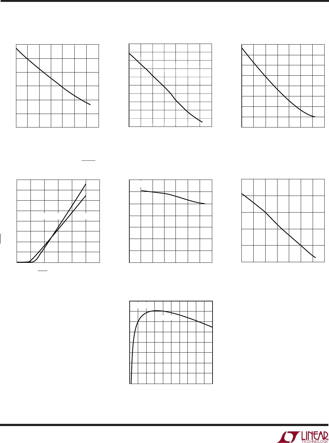
TYPICAL PERFOR A CE CHARACTERISTICS
UW
V.11 Mode I
CC
vs Data Rate
DATA RATE (kBd)
10
I
CC
(mA)
120
130
140
2846 G04
110
100
90
100 1000
150
160
170
10000
T
A
= 25°C
DATA RATE (kBd)
10
120
I
CC
(mA)
125
130
135
140
150
100 1000
2846 G05
10000
145
T
A
= 25°C
DATA RATE (kBd)
10
30
I
CC
(mA)
35
40
45
50
60
20 40 60 80 100
2846 G06
55
T
A
= 25°C
V.35 Mode I
CC
vs Data Rate V.28 Mode I
CC
vs Data Rate
6
LTC2846
sn2846 2846fs
TYPICAL PERFOR A CE CHARACTERISTICS
UW
V.11 Mode I
CC
vs Temperature V.35 Mode I
CC
vs Temperature V.28 Mode I
CC
vs Temperature
TEMPERATURE (°C)
–40
I
CC
(mA)
100
105
110
20 60
2846 G07
95
90
–20 0
40 80 100
85
80
TEMPERATURE (°C)
–40
123.0
I
CC
(mA)
123.5
124.5
125.0
125.5
128.0
126.5
0
40
60
2846 G08
124.0
127.0
127.5
126.0
–20
20
80
100
TEMPERATURE (°C)
–40
I
CC
(mA)
37.0
20
3846 G09
35.5
34.5
–20 0 40
34.0
33.5
37.5
36.5
36.0
35.0
60 80 100
Boost Switching Regulator SHDN
Pin Current vs Voltage
SHDN PIN VOLTAGE (V)
0
SHDN PIN CURRENT (µA)
15
20
25
3
5
2846 G10
10
5
0
12 4
30
35
40
6
T
A
= 25°C
T
A
= 100°C
Boost Switching Regulator
Current Limit vs Duty Cycle
DUTY CYCLE (%)
10
0.8
1.0
1.4
40 60
2846 G11
0.6
0.4
20 30
50 70 80
0.2
0
1.2
CURRENT LIMIT (A)
T
A
= 25°C
Boost Switching Regulator
Oscillator Frequency
vs Temperature
TEMPERATURE (°C)
–40 –20
1.05
FREQUENCY (MHz)
1.15
1.30
0
40
60
2846 G12
1.10
1.25
1.20
20
80
100
LOAD CURRENT (mA)
0
EFFICIENCY (%)
90
85
80
75
70
65
60
55
50
400
2846 TA01b
10050 150 250 350 450
200
300
500
V
IN
= 3.3V
T
A
= 25°C
Efficiency vs Load Current

LTC2846IG#TRPBF

Mfr. #:
Manufacturer:
Analog Devices Inc.
Description:
RS-232 Interface IC 3.3V Multiprotocol CLK_DATA Xcvr
Lifecycle:
New from this manufacturer.
Delivery:
DHL FedEx Ups TNT EMS
Payment:
T/T Paypal Visa MoneyGram Western Union