DS687F5 13
CS5343/4
Draft
3/10/15
4.1.2 Master Mode Operation
As clock Master, the CS5343/4 generates LRCK and SCLK synchronously on-chip. Table 3 shows the
available sample rates and associated clock ratios in Master Mode.
4.1.2.1 Master Mode Speed Selection
During power-up in Master Mode, the LRCK and SCLK pins are inputs to configure speed mode and the
output clock ratio. The LRCK pin is pulled low internally to select Single-Speed Mode by default, but Dou-
ble-Speed Mode is accessed with a 10 k pull-up resistor from LRCK to VA as shown in Table 4. Simi-
larly, the SCLK pin is internally pulled-low by default to select a 256x/512x MCLK/LRCK ratio, but a
MCLK/LRCK ratio of 348x/768x is accessed with a 10 k pull-up resistor from SCLK to VA as shown in
Table 4. Following the power-up routine, the LRCK and SCLK pins become clock outputs.
4.1.3 Master Clock
The CS5343/4 requires a Master clock (MCLK) which runs the internal sampling circuits and digital filters.
There is an internal automatic MCLK divider which is activated based on the input frequency of MCLK.
This divider selection allows the high and low MCLK speeds in a given speed mode (i.e. 256x and 512x
in SSM). Table 4 lists some common audio output sample rates and the required MCLK frequency.
Speed Mode
MCLK/LRCK
Ratio
SCLK/LRCK
Ratio
Input Sample Rate Range (kHz)
Single-Speed Mode
256x 64 4 - 24, 43 - 54
512x 64 43 - 54
384x 64 4 - 24, 43 - 54
768x 64 43 - 54
Double-Speed Mode
128x 64 86 - 108
256x 64 86 - 108
192x 64 86 - 108
384x 64 86 - 108
Table 3. Speed Modes and the Associated Sample Rates (Fs) in Master Mode
Pin Resistor Option Clock Configuration
LRCK
Internal Pull-Down to GND (100 k) Single-Speed Mode (default)
External Pull-Up to VA (10 k) Double-Speed Mode
SCLK
Internal Pull-Down to GND (100 k) 128x/256x/512x MCLK/LRCK (default)
External Pull-Up to VA (10 k) 192x/384x/768x MCLK/LRCK
Table 4. Speed Mode Selection in Master Mode
Master and Slave Mode
Sample Rate (kHz) Speed Mode
MCLK(MHz) MCLK (MHz)
256x 512x 384x 768x
32 (*Slave Mode Only) SSM *8.192 *16.384 *12.288 *24.576
44.1 SSM 11.289 22.579 16.934 33.868
48 SSM 12.288 24.576 18.432 36.864
Sample Rate (kHz) Speed Mode
MCLK(MHz) MCLK (MHz)
128x 256x 192x 384x
88.2 DSM 11.289 22.579 16.934 33.868
96 DSM 12.288 24.576 18.432 36.864
Table 5. Common MCLK Frequencies in Master and Slave Modes
14 DS687F5
CS5343/4
Draft
3/10/15
4.2 Serial Audio Interface
The CS5343 output is serial data in I²S audio format and the CS5344 output is serial data in Left-Justified
audio format. Figures 4 and 5 show the I²S and Left-Justified data relative to SCLK and LRCK. Additionally,
Figures 1 and 2 display more information on the required timing for the serial audio interface format. For an
overview of serial audio interface formats, please refer to Cirrus Application Note AN282.
4.3 Digital Interface
VA supplies power to both the analog and digital sections of the ADC, and also powers the serial port. Con-
sequently, the digital interface logic level must equal VA to within the limits specified under “Digital Charac-
teristics” on page 8.
4.4 Analog Connections
The analog modulator samples the input signal at half of the internal master clock rate, or 6.144 MHz when
MCLK = 12.288 MHz. The digital filter will reject signals within the stopband of the filter. However, there is
no rejection for input signals which are multiples of the input sampling frequency (n
6.144 MHz), where
n=0,1,2,... Refer to Figure 6 which shows the recommended topology of the analog input network. The ex-
ternal shunt capacitor and internal input impedance form a single-pole RC filter to provide the appropriate
filtering of noise at the modulator sampling frequency. Additionally, the 180 pF capacitor acts as a charge
source for the internal sampling circuits. Capacitors of NPO or other high-quality dielectric will produce the
best results while capacitors with a large voltage coefficient (such as general-purpose ceramics) can de-
grade signal linearity.
Figure 4. CS5343 I²S Serial Audio Interface
SDATA 23 22 8 7 23 22
SCLK
LRCK
23 226543210 8765432109 9
Left Channel Right Channel
Figure 5. CS5344 Left-Justified Serial Audio Interface
SDATA 23 22 7 6 23 22
SCLK
LRCK
23 225432108 7654321089 9
Left Channel Right Channel
Figure 6. CS5343/4 Analog Input Network
CS5343/4
AIN
Input
R1
R2
1 µF
180pF
C0G
DS687F5 15
CS5343/4
Draft
3/10/15
4.4.1 Component Values
Three parameters determine the values of resistors R1 and R2 as shown in Figure 6: source impedance,
attenuation, and input impedance. Table 6 shows the design equation used to determine these values.
Source Impedance: Source impedance is defined as the impedance as seen from the ADC looking
back into the signal network. The ADC achieves optimal THD+N performance with a source imped-
ance less than or equal to 2.5 k.
Attenuation: The required attenuation factor depends on the magnitude of the input signal. The full-
scale input voltage is specified under “Analog Characteristics - Commercial Grade (-CZZ)” on page 5.
The user should select values for R1 and R2 such that the magnitude of the incoming signal multiplied
by the attenuation factor is less than or equal to the full-scale input voltage of the device.
Input Impedance: Input impedance is the impedance from the signal source to the ADC analog input
pins, including the ADC. Because the ADC’s input impedance (see the “Analog Characteristics - Com-
mercial Grade (-CZZ)” table on page 5) is several orders of magnitude larger than the resistor values
typically used for the input attenuator, its contribution can be neglected when calculating the input im-
pedance. Table 6 shows the input parameters and the associated design equations for the input at-
tenuator.
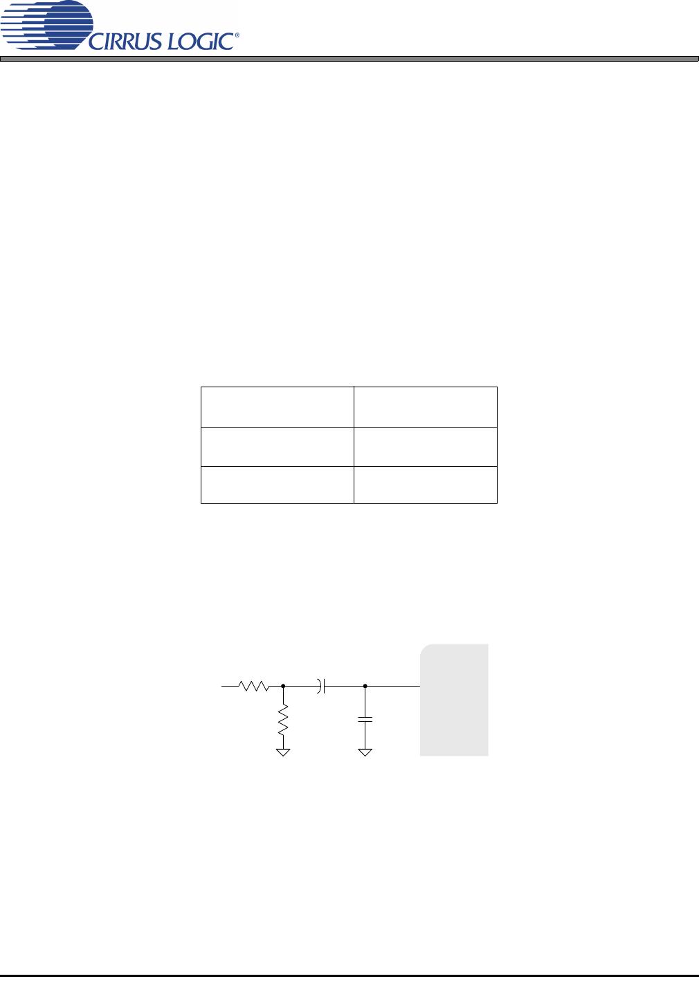
Figure 7 illustrates an example configuration using two 4.99 kresistors in place of R1 and R2. Based on
the discussion above, this circuit provides an optimal interface for both the ADC and the signal source.
First, consumer equipment frequently requires an input impedance of 10 kwhich the 4.99 kresistors
provide. Second, this circuit will attenuate a typical line level voltage, 2 Vrms, to the full-scale input of the
ADC, 1 Vrms when VA = 5 V. Finally, at 2.5 kthe source impedance optimizes analog performance of
the ADC.
4.5 Grounding and Power Supply Decoupling
As with any high-resolution converter, designing with the CS5343/4 requires careful attention to power sup-
ply and grounding arrangements if its potential performance is to be realized. Figure 3 shows the recom-
mended power arrangements, with VA connected to a clean supply. Decoupling capacitors should be as
near to the ADC as possible, with the low value ceramic capacitor being the nearest. All signals, especially
clocks, should be kept away from the FILT+ and VQ pins in order to avoid unwanted coupling into the mod-
ulators. The FILT+ and VQ decoupling capacitors, particularly the 0.1 µF, must be positioned to minimize
the electrical path from FILT+ to GND. The CDB5343 evaluation board demonstrates the optimum layout
and power supply arrangements. To minimize digital noise, connect the ADC digital outputs only to CMOS
inputs.
Source Impedance
Attenuation Factor
Input Impedance
Table 6. Analog Input Design Parameters
R1 R2
R1 R2+
------------------------ -
R2
R1 R2+
-------------------------
R1 R2+
Figure 7. CS5343/4 Example Analog Input Network
CS5343/4
AIN
Input
4.99 k
4.99 k
1 µF
180pF
C0G

CS5343-CZZR

Mfr. #:
Manufacturer:
Cirrus Logic
Description:
Audio A/D Converter ICs IC 98dB 24-bit 96kHz Stereo ADC
Lifecycle:
New from this manufacturer.
Delivery:
DHL FedEx Ups TNT EMS
Payment:
T/T Paypal Visa MoneyGram Western Union

Products related to this Datasheet