October 1987
Revised January 1999
MM74C911 4-Digit Expandable Segment Display Controller
© 1999 Fairchild Semiconductor Corporation DS005915.prf www.fairchildsemi.com
MM74C911
4-Digit Expandable Segment Display Controller
General Description
The MM74C911 display controller is an interface element
with memory that drives a 4-digit, 8-segment LED display.
The MM74C911 allows individual control of any segment in
the 4-digit display. The number of segments per digit can
be expanded without any external components. For exam-
ple, two MM74C911’s can be cascaded to drive a 16-seg-
ment alpha-numeric display.
The display controllers receive data information through 8
data lines a, b…DP, and digit information through 2
address inputs K1 and K2. The input data is written into the
register selected by the address information when CHIP
ENABLE, CE, and WRITE ENABLE, WE, are LOW and is
latched when either CE
or WE return HIGH. Data hold time
is not required.
A self-contained internal oscillator sequentially presents
the stored data to high drive (100 mA typ.) 3-STATE output
drivers which directly drive the LED display. The drivers are
active when the control pin labeled SEGMENT OUTPUT
ENABLE, SOE, is LOW and go into 3-STATE when SOE is
HIGH. This feature allows for duty cycle brightness control,
or for disabling the output drive for power conservation.
The digit outputs directly drive the base of the digit transis-
tor when the control pin labeled DIGIT INPUT OUTPUT
,
DIO
, is LOW. When DIO is HIGH, the digit lines turn into
inputs and the internal scanning multiplexer is disabled.
When any digit line is forced HIGH by an external device,
usually another MM74C911, the data information for that
digit is presented to the output. In this manner, 16-segment
alpha-numeric displays, 24- or 32-segment displays, or an
array of discrete LED's can be controlled by the simple cas-
cading of expandable segment display controllers. All
inputs except digit inputs are TTL compatible and do not
clamp input voltages above V
CC
.
Features
■ Direct segment drive (100 mA typ.) 3-STATE
■ 4 registers addressed like RAM
■ Internal oscillator and scanning circuit
■ Direct base drive to digit transistor
■ Segment expandability without external components
■ TTL compatible inputs
■ Power saver mode—5 µW (typ.)
Ordering Code:
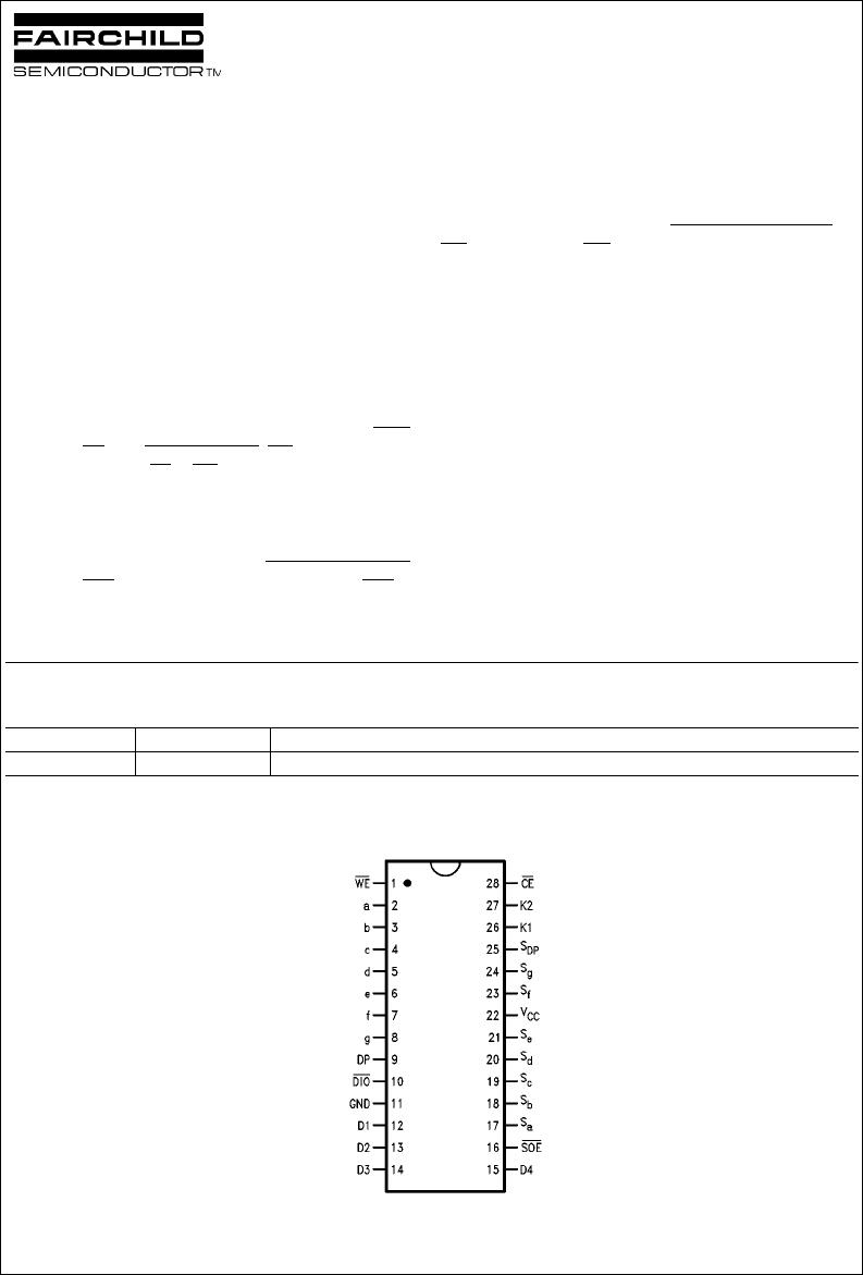
Connection Diagram
Pin Assignments for DIP
Top View
Order Number Package Number Package Description
MM74C991N N28B 28-Lead Plastic Dual-In-Line Package (PDIP), JEDEC MS−010, 0.600” Wide