www.fairchildsemi.com 4
MM74C911
AC Electrical Characteristics (Note 4)
V
CC
= 5V, t
r
= t
f
= 20 ns, C
L
= 50 pF
Note 4: AC Parameters are guaranteed by DC correlated testing.
Note 5: Capacitance guaranteed by periodic testing.
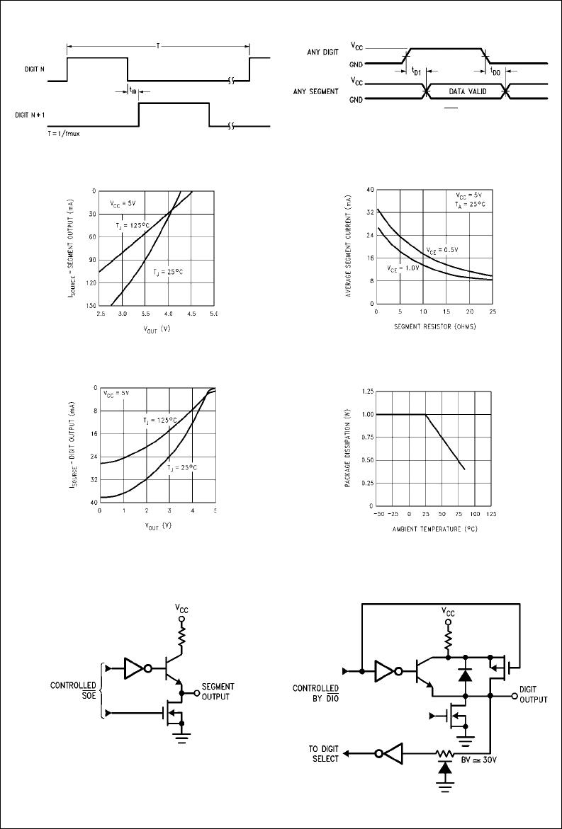
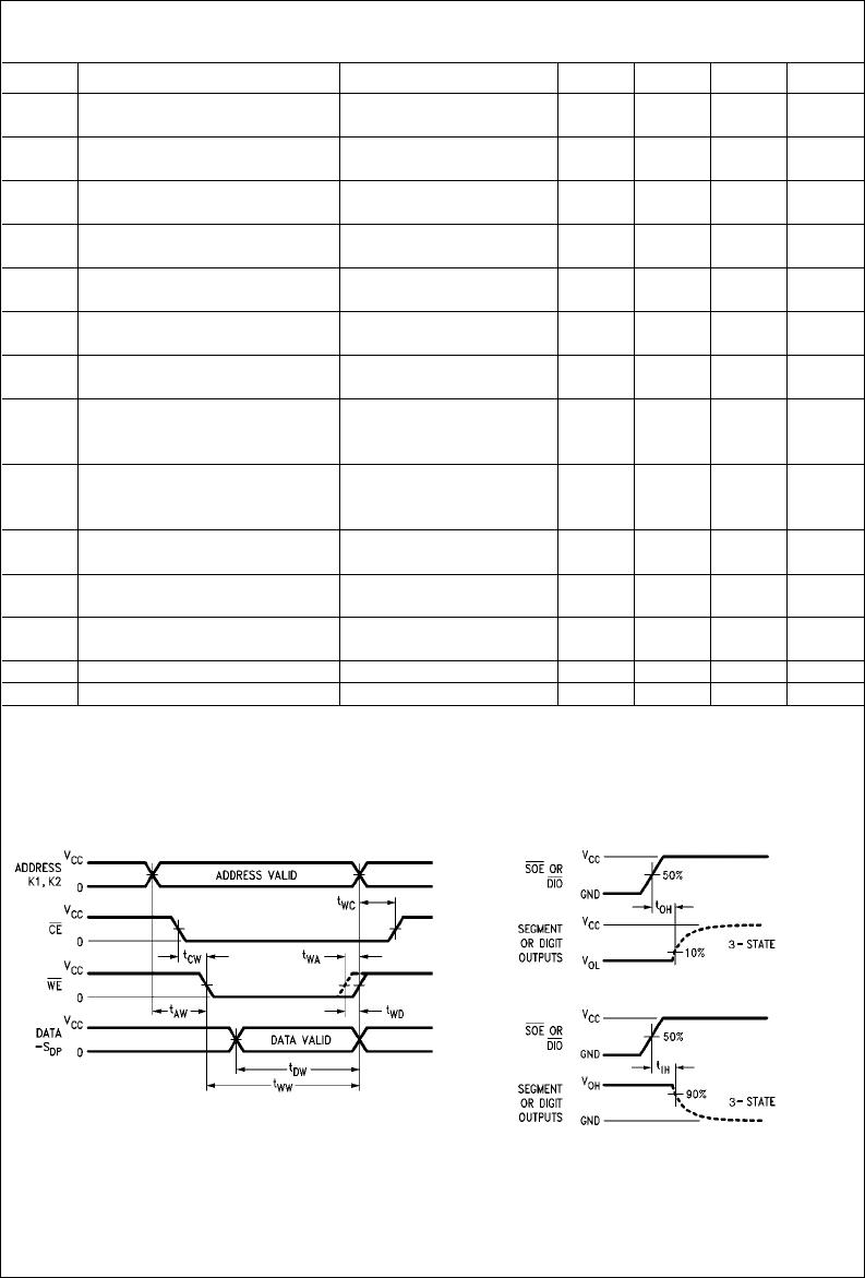
Switching Time Waveforms
Write Data Waveforms 3-STATE Waveforms
Symbol Parameter Conditions Min Typ Max Units
t
CW
Chip Enable to Write Enable Set-Up Time T
J
= 25°C3515ns
T
J
= 125°C5020ns
t
AW
Address to Write Enable Set-Up Time T
J
= 25°C3515ns
T
J
= 125°C5020ns
t
WW
Write Enable Width T
J
= 25°C 400 225 ns
T
J
= 125°C 450 250 ns
t
DW
Data to Write Enable Set-Up Time T
J
= 25°C 390 225 ns
T
J
= 125°C 430 250 ns
t
WD
Write Enable to Data Hold Time T
J
= 25°C0−10 ns
T
J
= 125°C0−15 ns
t
WA
Write Enable to Address Hold Time T
J
= 25°C0−10 ns
T
J
= 125°C0−15 ns
t
WC
Write Enable to Chip Enable Hold Time T
J
= 25°C5530ns
T
J
= 125°C7540ns
t
1H
, t
0H
Logical “1”, Logical “0” Levels into 3-STATE R
L
=10k, C
L
=10 pF
T
J
= 25°C 275 500 ns
T
J
= 125°C 325 600 ns
t
H1
, t
H0
3-STATE to Logical “1” or R
L
=10k, C
L
=10 pF
Logical “0” Levels T
J
= 25°C 325 600 ns
T
J
= 125°C 375 700 ns
t
D1
, t
D0
Propagation Delay from Digit Input to T
J
= 25°C 500 1000 ns
Segment Output T
J
= 125°C 700 1400 ns
t
IB
Interdigit Blanking Time T
J
= 25°C510µs
T
J
= 125°C1020µs
f
MUX
Multiplex Scan Frequency T
J
= 25°C525Hz
T
J
= 125°C375Hz
C
IN
Input Capacitance (Note 5) 5 7.5 pF
C
OUT
3-STATE Output Capacitance (Note 5) 30 50 pF