Intel MAX 10 Devices I/O Resources Per Package
Table 5. Package Plan for Intel MAX 10 Single Power Supply Devices
Device Package
Type M153
153-pin MBGA
U169
169-pin UBGA
U324
324-pin UBGA
E144
144-pin EQFP
Size 8 mm × 8 mm 11 mm × 11 mm 15 mm × 15 mm 22 mm × 22 mm
Ball Pitch 0.5 mm 0.8 mm 0.8 mm 0.5 mm
10M02 112 130 246 101
10M04 112 130 246 101
10M08 112 130 246 101
10M16 130 246 101
10M25 101
10M40 101
10M50 101
Table 6. Package Plan for Intel MAX 10 Dual Power Supply Devices
Device Package
Type V36
36-pin WLCSP
V81
81-pin WLCSP
U324
324-pin UBGA
F256
256-pin FBGA
F484
484-pin FBGA
F672
672-pin FBGA
Size 3 mm × 3 mm 4 mm × 4 mm 15 mm × 15
mm
17 mm × 17
mm
23 mm × 23
mm
27 mm × 27
mm
Ball Pitch 0.4 mm 0.4 mm 0.8 mm 1.0 mm 1.0 mm 1.0 mm
10M02 27 160
10M04 246 178
10M08 56 246 178 250
10M16 246 178 320
10M25 178 360
10M40 178 360 500
10M50 178 360 500
Related Links
Intel MAX 10 General Purpose I/O User Guide
Intel MAX 10 High-Speed LVDS I/O User Guide
Intel MAX 10 Vertical Migration Support
Vertical migration supports the migration of your design to other Intel MAX 10 devices
of different densities in the same package with similar I/O and ADC resources.
Intel
®
MAX
®
10 FPGA Device Overview
M10-OVERVIEW | 2017.12.15
Intel
®
MAX
®
10 FPGA Device Overview
7
Intel MAX 10 I/O Vertical Migration Support
Figure 2. Migration Capability Across Intel MAX 10 Devices
The arrows indicate the migration paths. The devices included in each vertical migration path are shaded.
Non-migratable devices are omitted. Some packages have several migration paths. Devices with lesser
I/O resources in the same path have lighter shades.
To achieve the full I/O migration across product lines in the same migration path, restrict I/Os usage to
match the product line with the lowest I/O count.
Device
V36 V81 M153 U169 U324 F256 E144 F484 F672
10M02
10M04
10M08
10M16
10M25
10M40
10M50
Package
Single Power Supply Devices
Dual Power Supply Devices
Note: To verify the pin migration compatibility, use the Pin Migration View window in the
Intel Quartus Prime software Pin Planner.
Intel MAX 10 ADC Vertical Migration Support
Figure 3. ADC Vertical Migration Across Intel MAX 10 Devices
The arrows indicate the ADC migration paths. The devices included in each vertical migration path are shaded.
Device
Package
M153 U169 U324 F256 E144 F484 F672
10M04
10M08
10M16
10M25
10M40
10M50
Dual ADC Device: Each ADC (ADC1 and ADC2) supports 1 dedicated analog input pin and 8 dual function pins.
Single ADC Device: Single ADC that supports 1 dedicated analog input pin and 16 dual function pins.
Single ADC Device: Single ADC that supports 1 dedicated analog input pin and 8 dual function pins.
Intel
®
MAX
®
10 FPGA Device Overview
M10-OVERVIEW | 2017.12.15
Intel
®
MAX
®
10 FPGA Device Overview
8
Table 7. Pin Migration Conditions for ADC Migration
Source Target Migratable Pins
Single ADC device Single ADC device You can migrate all ADC input pins
Dual ADC device Dual ADC device
Single ADC device Dual ADC device One dedicated analog input pin.
Eight dual function pins from the ADC1 block of the
source device to the ADC1 block of the target device.
Dual ADC device Single ADC device
Logic Elements and Logic Array Blocks
The LAB consists of 16 logic elements (LE) and a LAB-wide control block. An LE is the
smallest unit of logic in the Intel MAX 10 device architecture. Each LE has four inputs,
a four-input look-up table (LUT), a register, and output logic. The four-input LUT is a
function generator that can implement any function with four variables.
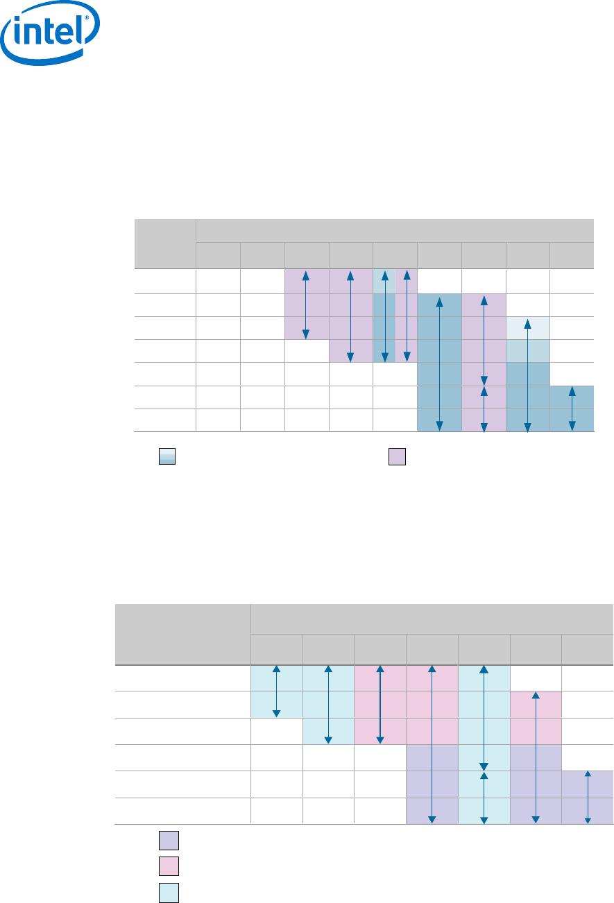
Figure 4. Intel MAX 10 Device Family LEs
Row, column, and
direct link routing
data 1
data 2
data 3
data 4
labclr1
labclr2
Chip-wide reset
(DEV_CLRn)
labclk1
labclk2
labclkena1
labclkena2
LE carry-in
LAB-wide
synchronous load
LAB-Wide
synchronous clear
Row, column, and
direct link routing
Local routing
Register chain output
Register bypass
Programmable register
Register chain routing
from previous LE
LE Carry-Out
Register feedback
Synchronous
Load and
Clear Logic
Carry
Chain
Look-Up Table
(LUT)
Asynchronous
Clear Logic
Clock and
Clock Enable
Select
D
Q
ENA
CLRN
Analog-to-Digital Converter
Intel MAX 10 devices feature up to two ADCs. You can use the ADCs to monitor many
different signals, including on-chip temperature.
Table 8. ADC Features
Feature Description
12-bit resolution Translates analog signal to digital data for information processing, computing,
data transmission, and control systems
Provides a 12-bit digital representation of the observed analog signal
Up to 1 MSPS sampling rate Monitors single-ended external inputs with a cumulative sampling rate of 25
kilosamples per second to 1 MSPS in normal mode
continued...
Intel
®
MAX
®
10 FPGA Device Overview
M10-OVERVIEW | 2017.12.15
Intel
®
MAX
®
10 FPGA Device Overview
9

10M04SCU169I7G

Mfr. #:
Manufacturer:
Intel / Altera
Description:
FPGA - Field Programmable Gate Array non-volatile FPGA, 130 I/O, 169UBGA
Lifecycle:
New from this manufacturer.
Delivery:
DHL FedEx Ups TNT EMS
Payment:
T/T Paypal Visa MoneyGram Western Union