LTC1064-3
2
10643fa
PARAMETER CONDITIONS MIN TYP MAX UNITS
Passband Gain Referenced to 0dB, 1Hz to 1kHz ● –0.5 0.15 dB
Gain TempCo 0.0002 dB/°C
–3dB Frequency 50:1 (f
CLK
/f
–3dB
= 75) 26.67 kHz
100:1 (f
CLK
/f
–3dB
= 150) 13.34 kHz
Gain at –3dB Frequency Referenced to 0dB, f
IN
= 26.67/13.34kHz ● –3.8 –2.75 dB
Stopband Attenuation At 3f
–3dB
● –25 –29 dB
Stopband Attenuation At 5f
–3dB
● –56 –60 dB
Stopband Attenuation At 7f
–3dB
–84 dB
Input Frequency Range 100:1 0 <f
CLK
/2 kHz
50:1 0 <f
CLK
kHz
Output Voltage Swing and V
S
= ±2.37V ● ±1.1 V
Operating Input Voltage Range V
S
= ±5V ● ±3.1 V
V
S
= ±7.5V ● ±5V
Total Harmonic Distortion V
S
= ±5V, Input = 1V
RMS
at 1kHz 0.015 %
V
S
= ±7.5V, Input = 3V
RMS
at 1kHz 0.03 %
Wideband Noise V
S
= ±5V, Input = GND 1Hz – 1.99MHz 55 µV
RMS
V
S
= ±7.5V, Input = GND 1Hz – 1.99MHz 60 µV
RMS
(Note 1)
The ● denotes the specifications which apply over the full operating
temperature range, otherwise specifications are at T
A
= 25°C. V
S
= ±7.5V, 75:1, f
CLK
= 2MHz, R1 = 10k, TTL or CMOS clock input level
unless otherwise specified.
Consult LTC Marketing for parts specified with wider operating temperature ranges.
Total Supply Voltage (V
+
to V
–
) ............................ 16.5V
Power Dissipation.............................................. 400mW
Storage Temperature Range ................. –65°C to 150°C
Lead Temperature (Soldering, 10 sec).................. 300°C
Operating Temperature Range
LTC1064-3M (OBSOLETE) ............... –55°C to 125°C
LTC1064-3C ....................................... – 40°C to 85°C
Input Voltage ........................... (V
+
+0.3V) to V
–
–0.3V)
Burn-In Voltage ....................................................... 15V
ABSOLUTE AXI U RATI GS
WWWU
ORDER PART
NUMBER
LTC1064-3CSW
T
JMAX
= 150°C, θ
JA
= 90°C/W
LTC1064-3CN
ORDER PART
NUMBER
T
JMAX
= 110°C, θ
JA
= 70°C/W
LTC1064-3MJ
LTC1064-3CJ
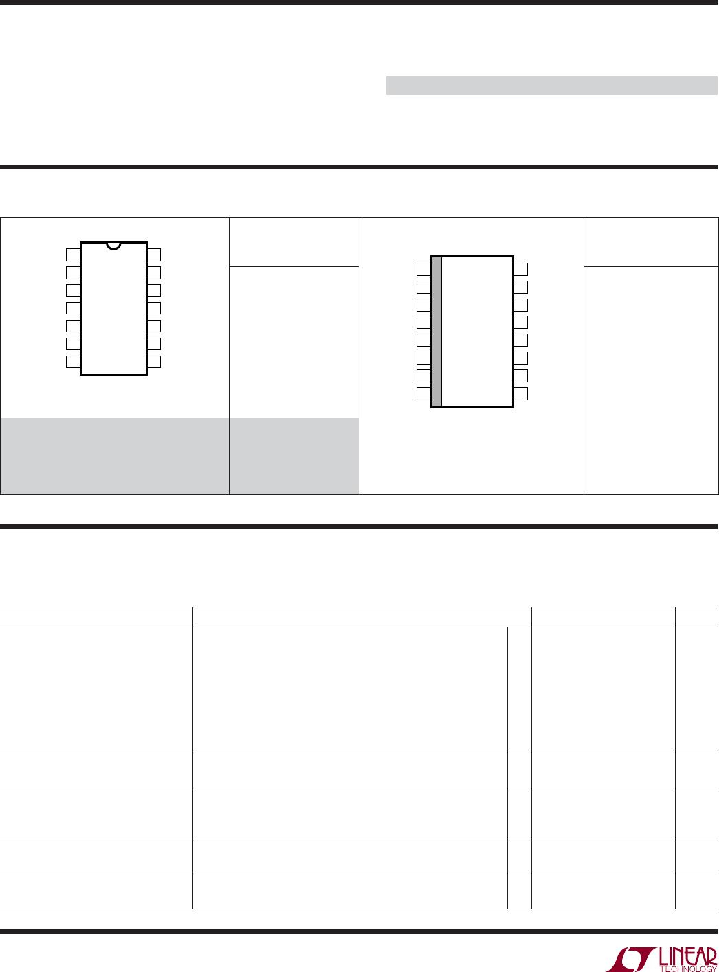
1
2
3
4
5
6
7
TOP VIEW
J PACKAGE
14-LEAD CERDIP
N PACKAGE
14-LEAD PDIP
14
13
12
11
10
9
8
NC
V
IN
AGND
V
+
AGND
NC
R
IN
A
OUT C
NC
V
–
f
CLK
75/150
V
OUT
NC
OBSOLETE PACKAGE
Consider the N 14 Package for Alternate Source
1
2
3
4
5
6
7
8
TOP VIEW
SW PACKAGE
16-LEAD PLASTIC (WIDE) SO
16
15
14
13
12
11
10
9
NC
V
IN
AGND
V
+
AGND
NC
NC
R
IN
A
OUT C
NC
V
–
NC
f
CLK
75/150
NC
V
OUT
PACKAGE/ORDER I FOR ATIO
UU
W
ELECTRICAL CHARACTERISTICS