LTC1064-3
7
10643fa
NC (Pins 1, 6, 8 and 13): The “no connection” pins should
be preferably grounded. These pins are not internally
connected.
V
IN
, V
OUT
(Pins 2, 9): The input Pin 2 is connected to an
18k resistor tied to the inverting input of an op amp. Pin 2
is protected against static discharge. The device’s output,
Pin 9, is the output of an op amp which can typically
source/sink 3mA/1mA. Although the internal op amps are
unity gain stable, driving long coax cables is not recom-
mended.
When testing the device for noise and distortion, the
output, Pin 9, should be buffered (Figure 1).
The op amp
power supply wire (or trace) should be connected
directly to the power source. To eliminate switching
transients from filter output, buffer filter output with a
third order lowpass (see Figure 5).
AGND (Pins 3, 5): For dual supply operation these pins
should be connected to a ground plane. For single supply
operation both pins should be tied to one half supply
(Figure 3).
V
+
, V
–
(Pins 4, 12): Should be bypassed with a 0.1µF
capacitor to an adequate analog ground. Low noise,
nonswitching power supplies are recommended.
To avoid
latchup when the power supplies exhibit high turn-on
transients, a 1N5817 Schottky diode should be added
from the V
+
and V
–
pins to ground (Figure 1, 2 and 3).
R
IN
A, OUT C (Pins 7, 14): A very short connection between
Pin 7 and Pin 14 is recommended. This connection should
be preferably done under the IC package. In a breadboard,
use a one inch, or less, shielded coaxial cable: the shield
should be grounded. In a PC board, use a one inch trace or
less; surround the trace by a ground plane.
50/100 (Pin 10): Ratio Pin.The DC level at this pin deter-
mines the ratio of clock frequency to the –3dB frequency of
the filter. The ratio is 75:1 when Pin 10 is at V
+
, 120:1 when
Pin 10 is at GND and 150:1 when Pin 10 is at V
–
. This pin
should be bypassed with a 0.1µF capacitor to analog
ground when it’s connected to V
–
or V
+
(Figure 1). See
Tables 2 through 8 for typical gain and delay responses for
the three ratios.
f
CLK
(Pin 11): For ±5V supplies the logic threshold level is
1.4V. For ±8V and 0V to 5V supplies the logic threshold
levels are 2.2V and 3V respectively. The logic threshold
levels vary ±100mV over the full military temperature
range. The recommended duty cycle of the input clock is
50% although for clock frequencies below 500kHz the
clock “on” time can be as low as 200ns. The maximum
clock frequency for ±5V supplies is 4MHz. For ±7V sup-
plies and above, the maximum clock frequency is 7MHz.
Do not allow the clock levels to exceed the power supplies.
For single supply operation ≥6V use level shifting at Pin 11
with T
2
L levels (see Figure 4).
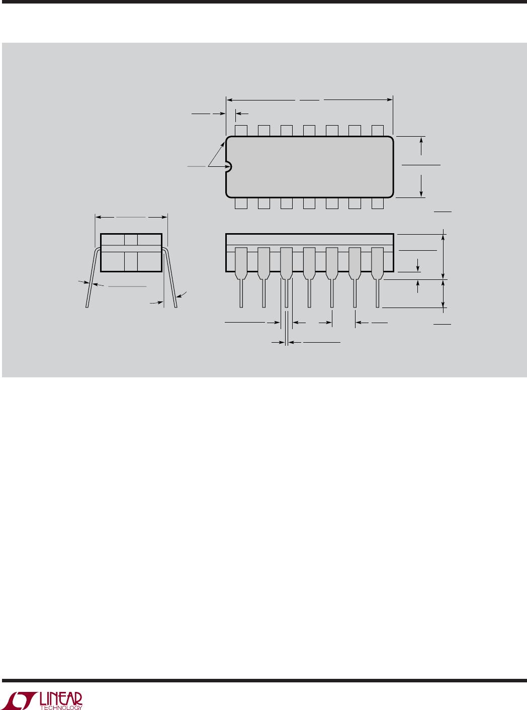
(Pin Numbers Refer to the 14-Pin Package)
UU
U
PI FU CTIO S