www.irf.com 4
IRF640N/S/LPbF
Fig 7. Typical Source-Drain Diode
Forward Voltage
Fig 5. Typical Capacitance Vs.
Drain-to-Source Voltage
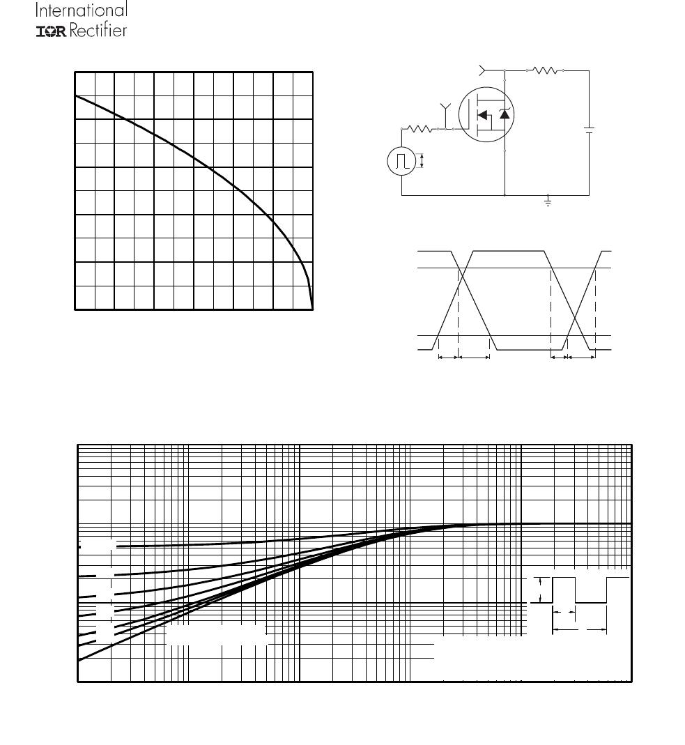
Fig 6. Typical Gate Charge Vs.
Gate-to-Source Voltage
0.1
1
10
100
1000
0.1 1 10 100 1000
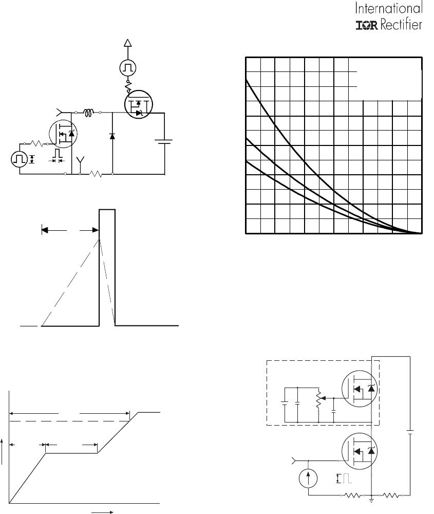
OPERATION IN THIS AREA LIMITED
BY R
DS(on)
Single Pulse
T
T
= 175 C
= 25 C
°
°
J
C
V , Drain-to-Source Voltage (V)
I , Drain Current (A)I , Drain Current (A)
DS
D
10us
100us
1ms
10ms
Fig 7. Typical Source-Drain Diode
Forward Voltage
Fig 8. Maximum Safe Operating Area
Fig 6. Typical Gate Charge Vs.
Gate-to-Source Voltage
1 10 100 1000
V
DS
, Drain-to-Source Voltage (V)
0
500
1000
1500
2000
2500
C
,
C
a
p
a
c
i
t
a
n
c
e
(
p
F
)
Coss
Crss
Ciss
V
GS
= 0V, f = 1 MHZ
C
iss
= C
gs
+ C
gd
, C
ds
SHORTED
C
rss
= C
gd
C
oss
= C
ds
+ C
gd
0 20 40 60 80
0
4
8
12
16
20
Q , Total Gate Charge (nC)
V , Gate-to-Source Voltage (V)
G
GS
I =
D
11A
V = 40V
DS
V = 100V
DS
V = 160V
DS
0.1
1
10
100
0.2 0.4 0.6 0.8 1.0 1.2 1.4 1.6
V ,Source-to-Drain Voltage (V)
I , Reverse Drain Current (A)
SD
SD
V = 0 V
GS
T = 25 C
J
°
T = 175 C
J
°