LTC1061
10
1061fe
f
IN
(kHz)
1.0
V
OUT
/V
IN
(dB)
–10
3.0
1061 F14
–30
–60
–80
1.5
2.0
2.5
3.5
–50
–40
–20
0
–70
–90
V
S
= ±5V
f
CLK
= 130kHz
R11 = 576k
R31 = 562k
R
h
11 = 28.7k
R22 = 10.7k
R42 = 10k
R
l
2 = 10k
R33 = 75k
R21 = 10k
R41 = 10.7k
R
l
11 = 40.2k
R32 = 562k
R
h
2 = 14k
R23 = 2.94k
NOTE: FOR CLOCK FREQUENCIES
ABOVE 500kHz, CONNECT A 5pF
IN PARALLEL WITH R41 AND R42.
STANDARD 1%
RESISTOR VALUES
f
IN
(kHz)
1.0
V
OUT
/V
IN
(dB)
–10
3.0
1061 F13
–30
–60
–70
1.5
2.0
2.5
3.5
–50
–40
–20
0
BW1
BW2
2.6kHz
STANDARD 1%
RESISTOR VALUES
R11 = 165k
R31 = 143k
R
h
1 = 10k
R22 = 20k
R42 = 15.4k
R
l
2 = 10k
R33 = 169k
R21 = 10k
R41 = 13k
R
l
1 = 10.5k
R32 = 221k
R
h
2 = 10.5k
R23 = 84.5k
NOTES: USE A 15pF CAPACITOR
BETWEEN PINS 17 AND 18.
PIN 7 IS GROUNDED.
V
S
= ±5V
f
CLK
= 260kHz
20
19
18
17
16
15
14
13
12
11
1
2
3
4
5
6
7
8
9
10
R32
V
IN
1061 F12
LTC1061
R22
R
h
2
R31
R41
R33
R23
T
2
L, CMOS
CLOCK INPUT
V
R42
V
+
NOTES: FOR NOTCH RESPONSES, PIN 7 SHOULD BE
PREFERABLY CONNECTED TO GROUND AND THE
FILTER OUTPUT IS PIN 3.
FOR BANDPASS OR LOWPASS RESPONSES, PIN 7
CAN BE EITHER AT GROUND OR POSITIVE SUPPLY,
AND THE FILTER OUTPUT IS PIN 2 OR PIN 1.
R
l
2
R
l
1
R21
R11
R
h
1
ODES OF OPERATIO
W
U
center frequencies, Qs, and notch frequencies are (f
O1
=
0.969, Q1 = 54.3, f
n1
= 0.84, f
O2
= 1.031, Q2 = 54.3, f
n2
=
1.187, f
O3
= 1, Q3 = 26.2). The output of the filter is the BP
output of Side A, Pin 2.
Lowpass filters with stopband notches can also be realized
by using Figure 12 provided that 6th order lowpass filter
approximations with 2 stopband notches can be synthe-
sized. Literature describing elliptic double terminated (RLC)
Figure 14. Resistor Values and Amplitude Response of Figure 12
Topology. The Bandpass Filter is Centered Around 2600Hz when
Operating with a 130kHz Clock.
Figure 13. Resistor Values and Amplitude Response of
Figure 12 Topology. The Notch is Centered at 2600Hz.
Figure 12. 6th Order Elliptic Bandpass, Lowpass
or Notch Topology
Figure 13 shows the measured frequency response of the
circuit Figure 12 configured to provide a notch function.
The filter output is taken out of pin 3. The resistor values
are standard 1%.
The ratio of the 0dB width, BW1, to the notch width BW2,
is 5:1 and matches the theoretical design value. The
measured notch depth was –53dB versus –56dB theoreti-
cal and the clock-to-center notch frequency ratio is 100:1.
Figure 14 shows the measured frequency response of the
circuit topology, Figure 12, but with pole/zero locations
configured to provide a high Q, 6th order elliptic bandpass
filter operating with a clock-to-center frequency ratio of
50:1 or 100:1. The theoretical passband ripple, stopband
attenuation and stopband to ripple bandwidth ratio are
0.5dB, 56dB, 5:1 respectively. The obtained results with
1% standard resistor values closely match the theoretical
frequency response. For this application, the normalized
11
LTC1061
1061fe
f
IN
(kHz)
0
V
OUT
/V
IN
(dB)
–10
2.0
1061 F17
–30
–60
–80
0.5
1.0
1.5
2.5
–50
–40
–20
0
–70
–90
f
CLK
= 250kHz
R11 = 105k
R31 = 47.5k
R
h
1 = 10k
R22 = 32.4k
R42 = 52.3k
R
l
2 = 750k
R33 = 255k
R
h
3 = 10k
R
g
= 140k
R21 = 10k
R41 = 45.3k
R
l
1 = 1.07M
R32 = 28.7k
R
h
2 = 42.2k
R23 = 10k
R43 = 63.4k
R
l
3 = 110k
NOTE: FOR CLOCK FREQUENCIES
BELOW 500kHz, USE A CAPACI-
TOR IN PARALLEL WITH R21
SUCH AS (1/2πR21C) f
CLK
/3.
STANDARD 1%
RESISTOR VALUES
20
19
18
17
16
15
14
13
12
11
1
2
3
4
5
6
7
8
9
10
V
IN
1061 F16
LTC1061
R
h
2
R43
R33
T
2
L
l
, CMOS
CLOCK INPUT
V
V
+
R
l
2
R32
R22
R42
R31
R41
R
l
1
R21
R11
R
h
1
R
l
3
R
h
3
R23
+
V
OUT
R
g
LT1056
f
IN
(kHz)
1
V
OUT
/V
IN
(dB)
–10
9
1061 F15
–30
–60
–80
3
5
7
0
–50
–40
–20
0
–70
–90
2
4
6810
STANDARD 1%
RESISTOR VALUES
R11 = 39.2k
R31 = 13.7k
R
h
1 = 20.5k
R22 = 10k
R42 = 14k
R
l
2 = 11.8k
R33 = 100k
R21 = 10k
R41 = 39.2k
R
l
1 = 12.4k
R32 = 26.7k
R
h
2 = 32.4k
R23 = 10k
NOTES: USE A 10pF ACROSS R42
FOR f
CLK
> 1MHz.
THE ELLIPTIC LOWPASS FILTER
HAS ONLY TWO NOTCHES IN THE
STOPBAND, AND IT OPERATES
WITH A CLOCK TO CUTOFF
FREQUENCY RATIO OF 50:1.
Figure 17. Measured Amplitude Response of the Topology of
Figure 16, Configured to Provide a 6th Order Elliptic Highpass
Filter Operating with a Clock-to-Cutoff Frequency Ratio of 250:1
ODES OF OPERATIO
W
U
Figure 15. Resistor Values and Amplitude Response of
the Topology of Figure 12
passive ladder filters provide enough data to synthesize
the above filters. The measured amplitude response of
such a lowpass is shown in Figure 15 where the filter
output is taken out of side A’s Pin 1, Figure 12. The clock-
to-center frequency ratio can be either 50:1 or 100:1
because the last stage of the LTC1061 operates in Mode 1
with a center frequency very close to the overall cutoff
frequency of the lowpass filter.
In Figure 16, all three sides of the LTC1061 are connected
in Mode 3a. This topology is useful for elliptic highpass
and notch filters with clock-to-cutoff (or notch) frequency
ratio higher than 100:1. This is often required to extend the
allowed input signal frequency range and to avoid prema-
ture aliasing. Figure 16 is also a versatile, general purpose
architecture providing 3 notches and 4 pole pairs, and
there is no restriction on the location of the poles with
respect to the notch frequencies. The drawbacks, when
compared to Figure 12, are the use of an external op amp
and the increased number of the required external
resistors.
Figure 17 shows the measured frequency of a 6th order
highpass elliptic filter operating with 250:1 clock-to-cutoff
frequency ratio. With a 1MHz clock, for instance, the filter
yields a 4kHz cutoff frequency, thus allowing an input
frequency range beyond 100kHz. Band limiting can be
easily added by placing a capacitor across the feedback
resistor of the external op amp of Figure 16.
Figure 16. Using an External Op Amp to Connect
all 3 Sides of the LTC1061 in Mode 3a
LTC1061
12
1061fe
+
Σ
AGND
R1
N
BP
LP
V
IN
1061 F20
+
S
R2
R3
R4
f
O
= ; f
n
= ; Q =
H
OLP
= ; H
OBP
= –
H
ON1
(f 0) = ; H
ON2
= –
f
CLK
100(50)
R2
R1
R3
R2
–R2/R1
1 + (R2/R4)
R3
R1
f
CLK
2
f
()
1 +
R2
R4
f
CLK
100(50)
1 +
R2
R4
–R2/R1
1 + (R2/R4)
f
IN
(kHz)
1
0
V
OUT
/V
IN
(dB)
–90
–50
–30
–10
10 100
1061 F19
–80
–70
–60
–40
–20
4
STANDARD 1%
RESISTOR VALUES
R11 = 30.9k
R31 = 16.2k
R
h
1 = 45.3k
R22 = 10.5k
R42 = 10k
R
l
2 = 15.8k
R33 = 28.7k
R
h
3 = 95.3k
R
g
= 28k
R21 = 10k
R41 = 26.7k
R
l
1 = 19.6k
R32 = 100k
R
h
2 = 52.3k
R23 = 10k
R43 = 12.7k
R
l
3 = 10k
NOTE: ADD A CAPACITOR C ACROSS R
g
TO CREATE A 7TH ORDER
LOWPASS SUCH AS (1/2πR
g
C) = (CUTOFF FREQUENCY) × 0.38
f
CLK
200kHz
f
CLK
500kHz
f
CLK
1MHz
f
IN
(kHz)
0
V
OUT
/V
IN
(dB)
–10
1.6
1061 F18
–30
–60
–70
0.2
0.8
1.2
2.0
–50
–40
–20
0
f
CLK
= 250kHz
0.4 0.6
1.0 1.4 1.8
STANDARD 1%
RESISTOR VALUES
R11 = 84.5k
R31 = 31.6k
R
h
1 = 48.7k
R22 = 10k
R42 = 97.6k
R
l
2 = 66.5k
R33 = 300k
R
h
3 = 10.2k
R
g
= 210k
R21 = 10.2k
R41 = 63.4k
R
l
1 = 287k
R32 = 232k
R
h
2 = 10.2k
R23 = 20k
R43 = 80.6k
R
l
3 = 63.4k
NOTE: CONNECT 39pF AND
100pF ACROSS R21 AND R22
RESPECTIVELY.
ODES OF OPERATIO
W
U
Mode 2 – This is a combination of Mode 1 and Mode 3,
Figure 20. With Mode 2, the clock-to-center frequency
ratio, f
CLK
/f
O
, is always less than 50:1 or 100:1. When
compared to Mode 3 and for applications requiring 2nd
order section with f
CLK
/f
O
slightly less than 100 or 50:1,
Mode 2 provides less sensitivity to resistor tolerances. As
in Mode 1, Mode 2 has a notch output which directly
depends on the clock frequency and therefore the notch
frequency is always less than the center frequency, f
O
, of
the 2nd order section.
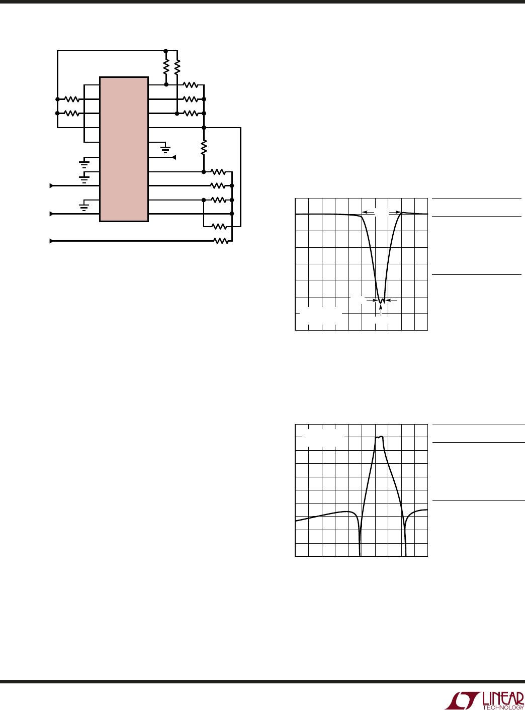
Figure 18 shows the plotted amplitude responses of a 6th
order notch filter operating again with a clock-to-center
notch frequency ratio of 250:1. The theoretical notch
depth is 70dB and when the notch is centered at 1kHz its
width is 50Hz. Two small, noncritical capacitors were used
across the R21 and R22 resistors of Figure 16, to band-
limit the first two highpass outputs such that the practical
notch depth will approach the theoretical value. With these
two fixed capacitors, the notch frequency can be swept
within a 3:1 range.
When the circuit of Figure 16 is used to realize lowpass
elliptic filters, a capacitor across R
g
raises the order of the
filter and at the same time eliminates any small clock
feedthrough. This is shown in Figure 19 where the ampli-
tude response of the filter is plotted for 3 different cutoff
frequencies. When the clock frequency equals or exceeds
1MHz, the stopband notches lose their depth due to the
finite bandwidth of the internal op amps and to the small
crosstalk between the different sides of the LTC1061. The
lowpass filter, however, does not lose its passband accu-
racy and it maintains nearly all of its attenuation slope. The
theoretical performance of the 7th order lowpass filter of
Figure 19 is 0.2dB passband ripple, 1.5:1 stopband-to-
cutoff frequency ratio, and 73dB stopband attenuation.
Without any tuning, the obtained results closely approxi-
mate the textbook response.
Figure 19. Frequency Responses of a 7th Order Lowpass Elliptic
Filter Realized with Figure 16 Topology
Figure 18. 6th Order Band Reject Filter Operating with a Clock-
to-Center Notch Frequency Ratio of 250:1. The Ratio of 0dB to
the –65dB Notch Width is 8:1.
Figure 20. Mode 2: 2nd Order Filter Providing
Notch, Bandpass, Lowpass

LTC1061CSW#PBF

Mfr. #:
Manufacturer:
Analog Devices Inc.
Description:
Active Filter Triple Switched Capacitor Filter
Lifecycle:
New from this manufacturer.
Delivery:
DHL FedEx Ups TNT EMS
Payment:
T/T Paypal Visa MoneyGram Western Union