13
LTC1061
1061fe
f
IN
(kHz)
1
V
OUT
/V
IN
(dB)
–10
9
1061 F22
–30
–60
–80
3
5
7
0
–50
–40
–20
0
–70
–90
2
4
6810
STANDARD 1%
RESISTOR VALUES
R11 = 54.9k
R31 = 34.8k
R
h
1 = 28.7k
R22 = 68.1k
R42 = 10k
R
l
2 = 16.2k
R33 = 75k
R21 = 24.3k
R41 = 10k
R
l
1 = 280k
R32 = 18.2k
R
h
2 = 10.2k
R23 = 10k
R43 = 14k
NOTE: FOR CLOCK FREQUEN-
CIES ABOVE 300kHz, ADD
A CAPACITOR C ACROSS
R21 AND R22 SUCH AS
(1/2πR21C) = f
CLK
20
19
18
17
16
15
14
13
12
11
1
2
3
4
5
6
7
8
9
10
V
IN
1061 F21
LTC1061
R
h
2
R43
R33
T
2
L, CMOS
CLOCK INPUT
V
V
+
R
l
2
R32
R22
R42
R31
R41
R
l
1
R21
R11
R
h
1
R23
V
OUT
ODES OF OPERATIO
W
U
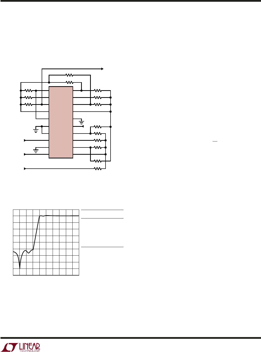
higher frequency notch provided by the side A of the
LTC1061. As shown in Figure 22, the highpass corner
frequency is 3.93kHz and the higher notch frequency is
3kHz while the filter operates with a 300kHz clock. The
center frequencies, Qs, and notches of Figure 22, when
normalized to the highpass cutoff frequency, are (f
O1
=
1.17, Q1 = 2.24, f
n1
= 0.242, f
O2
= 1.96, Q2 = 0.7, f
n2
= 0.6,
f
O3
= 0.987, f
n3
= 0.753, Q3 = 10). When compared with the
topology of Figure 16, this approach uses lower and more
restricted clock frequencies. The obtained notch in Mode
2 is shallower although the topology is more efficient.
Output Noise
The wideband RMS noise of the LTC1061 outputs is nearly
independent from the clock frequency. The LTC1061
noise when operating with ±2.5V supply is lower, as Table
3 indicates. The noise at the bandpass and lowpass
outputs increases rough as the Q. Also the noise in-
creases when the clock-to-center frequency ratio is al-
tered with external resistors to exceed the internally set
100:1 or 50:1 ratios. Under this condition, the noise
increases square root-wise.
Output Offsets
The equivalent input offsets of the LTC1061 are shown in
Figure 23. The DC offset at the filter bandpass output is
always equal to V
OS3
. The DC offsets at the remaining two
outputs (Notch and LP) depend on the mode of operation
and external resistor ratios. Table 4 illustrates this.
It is important to know the value of the DC output offsets,
especially when the filter handles input signals with large
dynamic range. As a rule of thumb, the output DC offsets
increase when:
1. The Qs decrease
2. The ratio (f
CLK
/f
O
) increases beyond 100:1. This is
done by decreasing either the (R2/R4) or the R6/(R5
+ R6) resistor ratios.
Figure 21 shows the side A of the LTC1061 connected in
Mode 2 while sides B and C are in Mode 3a. This topology
can be used to synthesize elliptic bandpass, highpass and
notch filters. The elliptic highpass of Figure 17 is synthe-
sized again, Figure 22, but the clock is now locked onto the
Figure 22. 6th Order Elliptic Highpass Filter Operating with a
Clock-to-Cutoff Frequency Ratio of 75:1 and Using the Topology
of Figure 21
Figure 21. LTC1061 with Side A is Connected in Mode 2 While
Side B, C are in Mode 3a. Topology is Useful for Elliptic
Highpass, Notch and Bandpass Filters.
LTC1061
14
1061fe
+
1061 F23
+
V
OS2
V
OS1
Σ
(12,18)
3
5
+
+
V
OS3
2
+
+
1
6
(13,19)
(14,20)
(11,17)
+
4
ODES OF OPERATIO
W
U
NOTCH/HP BP LP
V
S
(±V) f
CLK/
f
O
(µV
RMS
)(µV
RMS
)(µV
RMS
) CONDITIONS
5.0 50:1 45 55 70 Mode 1, R1 = R2 = R3
5.0 100:1 65 65 85 Q = 1
2.5 50:1 30 30 45
2.5 100:1 40 40 60
5.0 50:1 18 150 150 Mode 1, Q = 10
5.0 100:1 20 200 200 R1 = R3 for BP Out
2.5 50:1 15 100 100 R1 = R2 for LP Out
2.5 100:1 17 140 140
5.0 50:1 57 57 62 Mode 3, R1 = R2 = R3 = R4
5.0 100:1 72 72 80 Q = 1
2.5 50:1 40 40 42
2.5 100:1 50 50 53
5.0 50:1 135 120 140 Mode 3, R2 = R4, Q = 10
5.0 100:1 170 160 185 R3 = R1 for BP Out
2.5 50:1 100 88 100 R4 = R1 for LP and HP Out
2.5 100:1 125 115 130
Table 3. Wideband RMS Noise
Figure 23. Equivalent Input Offsets of 1/3 LTC1061 Filter Building Block
V
OSN
V
OSBP
V
OSLP
MODE PIN 3 (18) PIN 2 (19) PIN 1 (20)
1V
OS1
[(1/Q) + 1 + || H
OLP
||] – V
OS3
/Q V
OS3
V
OSN
V
OS2
1b V
OS1
[(1/Q) + 1 + R2/R1] – V
OS3
/Q V
OS3
~(V
OSN
V
OS2
)(1 + R5/R6)
2[V
OS1
(1 + R2/R1 + R2/R3 + R2/R4) – V
OS3
(R2/R3)] × V
OS3
V
OSN
V
OS2
× [R4/(R2 + R4)] + V
OS2
[R2/(R2 + R4)]
3V
OS2
V
OS3
V
OS1
(1 + R4/R1 + R4/R2 + R4/R3) – V
OS2
(R4/R2)
– V
OS3
(R4/R3)
Table 4
15
LTC1061
1061fe
N Package
20-Lead PDIP (Narrow .300 Inch)
(Reference LTC DWG # 05-08-1510)
OBSOLETE PACKAGE
J20 0801
3
7
56
109
1
42
8
11
20 16 1517 14 13 1219 18
.005
(0.127)
MIN
.025
(0.635)
RAD TYP
.220 – .310
(5.588 – 7.874)
1.060
(26.924)
MAX
0° – 15°
.008 – .018
(0.203 – 0.457)
.015 – .060
(0.381 – 1.524)
.125
(3.175)
MIN
.014 – .026
(0.356 – 0.660)
.045 – .065
(1.143 – 1.651)
.100
(2.54)
BSC
.200
(5.080)
MAX
.300 BSC
(7.62 BSC)
.045 – .065
(1.143 – 1.650)
FULL LEAD
OPTION
.023 – .045
(0.584 – 1.143)
HALF LEAD
OPTION
CORNER LEADS OPTION
(4 PLCS)
NOTE: LEAD DIMENSIONS APPLY TO SOLDER DIP/PLATE
OR TIN PLATE LEADS
Information furnished by Linear Technology Corporation is believed to be accurate and reliable.
However, no responsibility is assumed for its use. Linear Technology Corporation makes no represen-
tation that the interconnection of its circuits as described herein will not infringe on existing patent rights.
PACKAGE DESCRIPTIO
U
J Package
20-Lead CERDIP (Narrow .300 Inch, Hermetic)
(Reference LTC DWG # 05-08-1110)
N20 0405
.020
(0.508)
MIN
.120
(3.048)
MIN
.125 – .145
(3.175 – 3.683)
.065
(1.651)
TYP
.045 – .065
(1.143 – 1.651)
.018 ± .003
(0.457 ± 0.076)
.005
(0.127)
MIN
.255 ± .015*
(6.477 ± 0.381)
1.060*
(26.924)
MAX
12
3
4
5
6
7
8
910
19 1112
131416
1517
18
20
.008 – .015
(0.203 – 0.381)
.300 – .325
(7.620 – 8.255)
.325
+.035
–.015
+0.889
–0.381
8.255
()
NOTE:
1. DIMENSIONS ARE
INCHES
MILLIMETERS
*THESE DIMENSIONS DO NOT INCLUDE MOLD FLASH OR PROTRUSIONS.
MOLD FLASH OR PROTRUSIONS SHALL NOT EXCEED .010 INCH (0.254mm)
.100
(2.54)
BSC

LTC1061CSW#PBF

Mfr. #:
Manufacturer:
Analog Devices Inc.
Description:
Active Filter Triple Switched Capacitor Filter
Lifecycle:
New from this manufacturer.
Delivery:
DHL FedEx Ups TNT EMS
Payment:
T/T Paypal Visa MoneyGram Western Union