LTC1044A
8
1044afa
For more information www.linear.com/LTC1044A
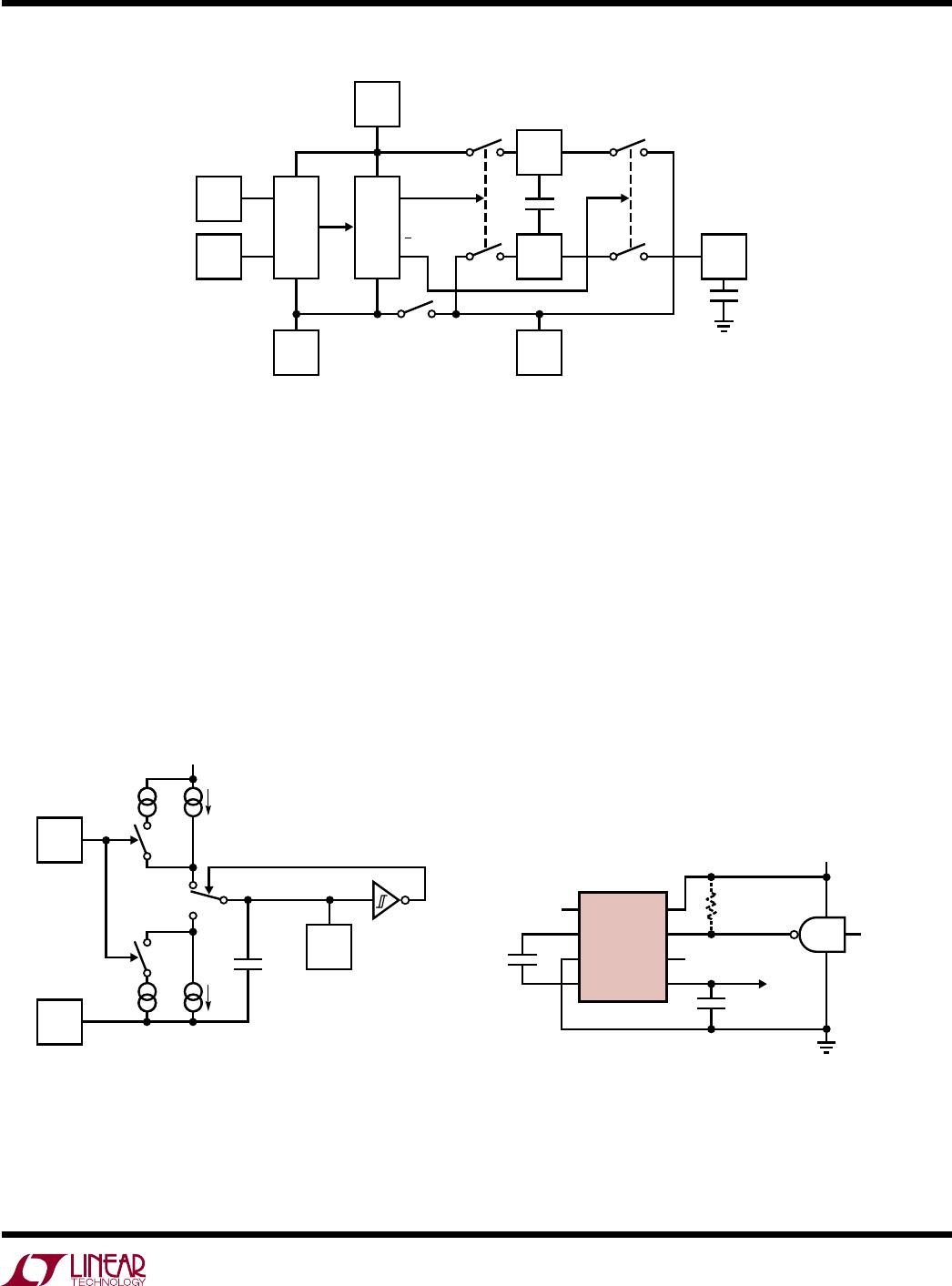
applicaTions inForMaTion
Capacitor Selection
External capacitors C1 and C2 are not critical. Matching is
not required, nor do they have to be high quality or tight
tolerance. Aluminum or tantalum electrolytics are excellent
choices with cost and size being the only consideration.
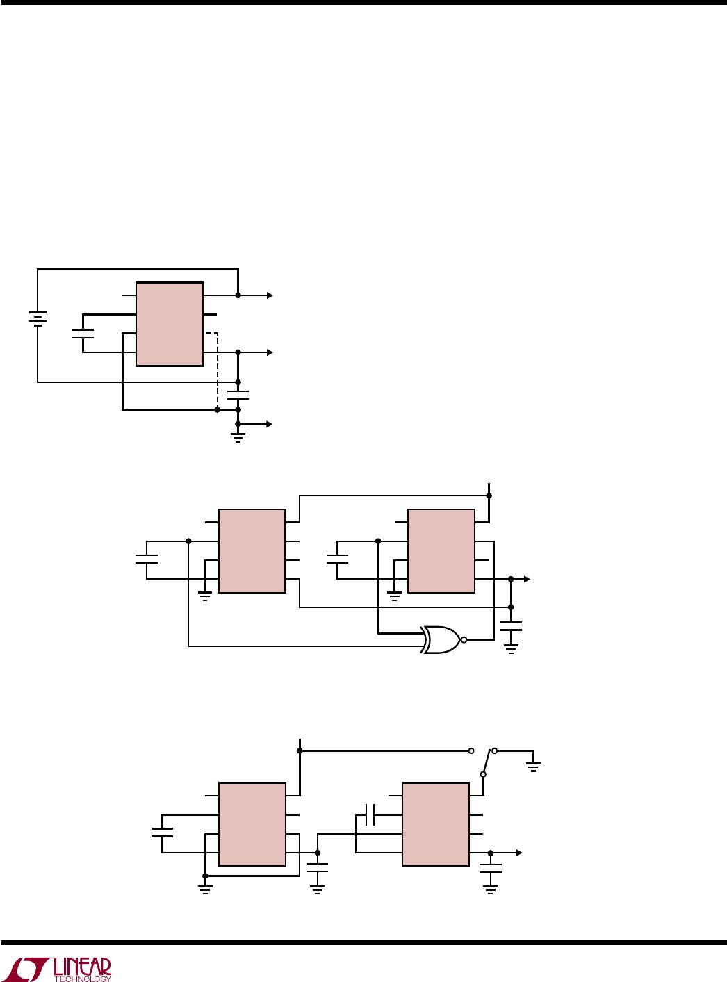
Negative Voltage Converter
Figure 6 shows a typical connection which will provide
a negative supply from an available positive supply. This
circuit operates over full temperature and power supply
ranges without the need of any external diodes. The LV
pin (pin 6) is shown grounded, but for V
+
≥ 3V it may be
floated, since LV is internally switched to ground (pin 3)
for V
+
≥ 3V.
The output voltage (pin 5) characteristics of the circuit
are those of a nearly ideal voltage source in series with
an 80Ω resistor. The 80Ω output impedance is composed
of two terms:
1. The equivalent switched-capacitor resistance (see
Theory of Operation).
2. A term related to the on-resistance of the MOS
switches.
At an oscillator frequency of 10kHz and C1 = 10µF, the
first term is:
R
EQUIV
=
(f
OSC
/ 2)• C1
=
1
3
– 6
=20Ω
Notice that the above equation for R
EQUIV
is not a capaci-
tive reactance
equation (X
C
= 1/C) and does not contain
a 2π term.
Figure 6. Negative Voltage Converter
The exact expression for output resistance is extremely
complex, but the dominant effect of the capacitor is
clearly shown on the typical curves of Output Resistance
and Power Efficiency vs Frequency. For C1 = C2 = 10µF,
the output impedance goes from 60Ω at f
OSC
= 10kHz to
200Ω at f
OSC
= 1kHz. As the 1/(f • C) term becomes large
compared to the switch-on resistance term, the output
resistance is determined by 1/(f • C) only.
Voltage Doubling
Figure 7 shows a two-diode capacitive voltage doubler.
With a 5V input, the output is 9.93V with no load and 9.13V
with a 10mA load. With a 10V input, the output is 19.93V
with no load and 19.28V with a 10mA load.
1
2
3
4
8
7
6
5
LTC1044A
V
OUT
= –V
+
REQUIRED FOR V
+
< 3V
V
+
(1.5V TO 12V)
T
MIN
≤ T
A
≤ T
MAX
+
+
10µF
10µF
1044a F06
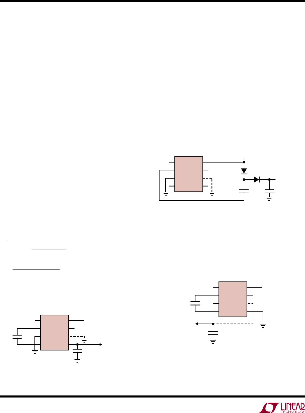
Ultra-Precision Voltage Divider
An ultra-precision voltage divider is shown in Figure 8. To
achieve the 0.002% accuracy indicated, the load current
should be kept below 100nA. However, with a slight loss
in accuracy the load current can be increased.
Figure 7. Voltage Doubler
1
2
3
4
8
7
6
5
LTC1044A
V
IN
(1.5V TO 12V)
V
OUT
= 2(V
IN
– 1)
V
d
1N5817
V
d
1N5817
REQUIRED
FOR V
+
< 3V
1044a F07
+
+
+
+
10µF 10µF
Figure 8. Ultra-Precision Voltage Divider
1
2
3
4
8
7
6
5
LTC1044A
V
+
(3V TO 24V)
+
C1
10µF
V
+
/2 ±0.002%
+
C2
10µF
REQUIRED FOR
V
+
< 6V
1044a F08
T
MIN
≤ T
A
≤ T
MAX
I
L
≤ 100nA