7SB3126MUTCG

© Semiconductor Components Industries, LLC, 2010
September, 2010 Rev. 1
1 Publication Order Number:
7SB3126/D
7SB3126
Bus Switch
The 7SB3126 Bus Switch is an advanced highspeed line switch in
ultrasmall footprint.
Features
High Speed: t
PD
= 0.25 ns (Max) @ V
CC
= 4.5 V
3 W Switch Connection Between 2 Ports
Power Down Protection Provided on Inputs
UltraSmall Packages
These are PbFree Devices
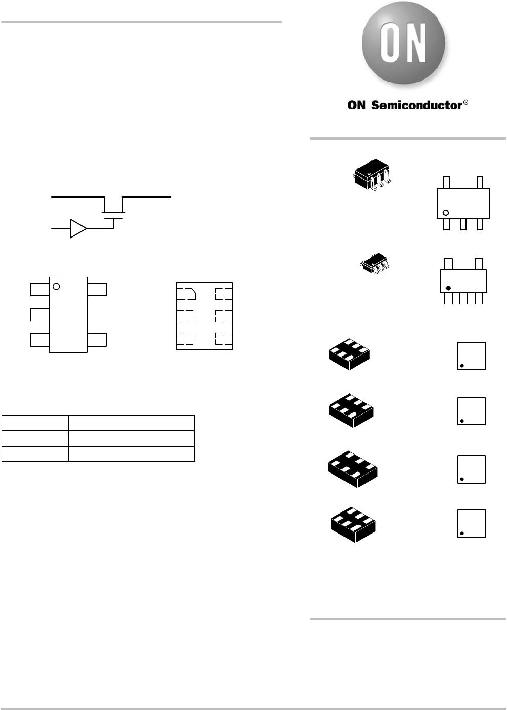
Figure 1. Logic Diagram
Figure 2. TSOP5/SC88A
(Top View)
BA
OE
OE
A
GND
V
CC
B
1
2
3
5
4
OE
A
GND
V
CC
B
NC
1
2
3
6
5
4
Figure 3. ULLGA6/UDFN6
(Top View)
Function Table
Input OE Function
L Disconnect
H B = A
See detailed ordering and shipping information in the package
dimensions section on page 4 of this data sheet.
ORDERING INFORMATION
MARKING
DIAGRAMS
http://onsemi.com
1
1
1
ULLGA6
1.0 x 1.0
CASE 613AD
ULLGA6
1.2 x 1.0
CASE 613AE
ULLGA6
1.45 x 1.0
CASE 613AF
J
M
1
5
1
5
AF MG
G
(Note: Microdot may be in either location)
AJ, AF, J, 6, A, K = Specific Device Code
M = Date Code
G = PbFree Package
SOT235/TSOP5/SC595
DT SUFFIX
CASE 483
SOT353/SC705/SC88A
DF SUFFIX
CASE 419A
1
5
AJ MG
G
G
M
G
M
G
1
5
UDFN6
1.2 x 1.0
CASE 517AA
K
M
G
1
6
A
7SB3126
http://onsemi.com
2
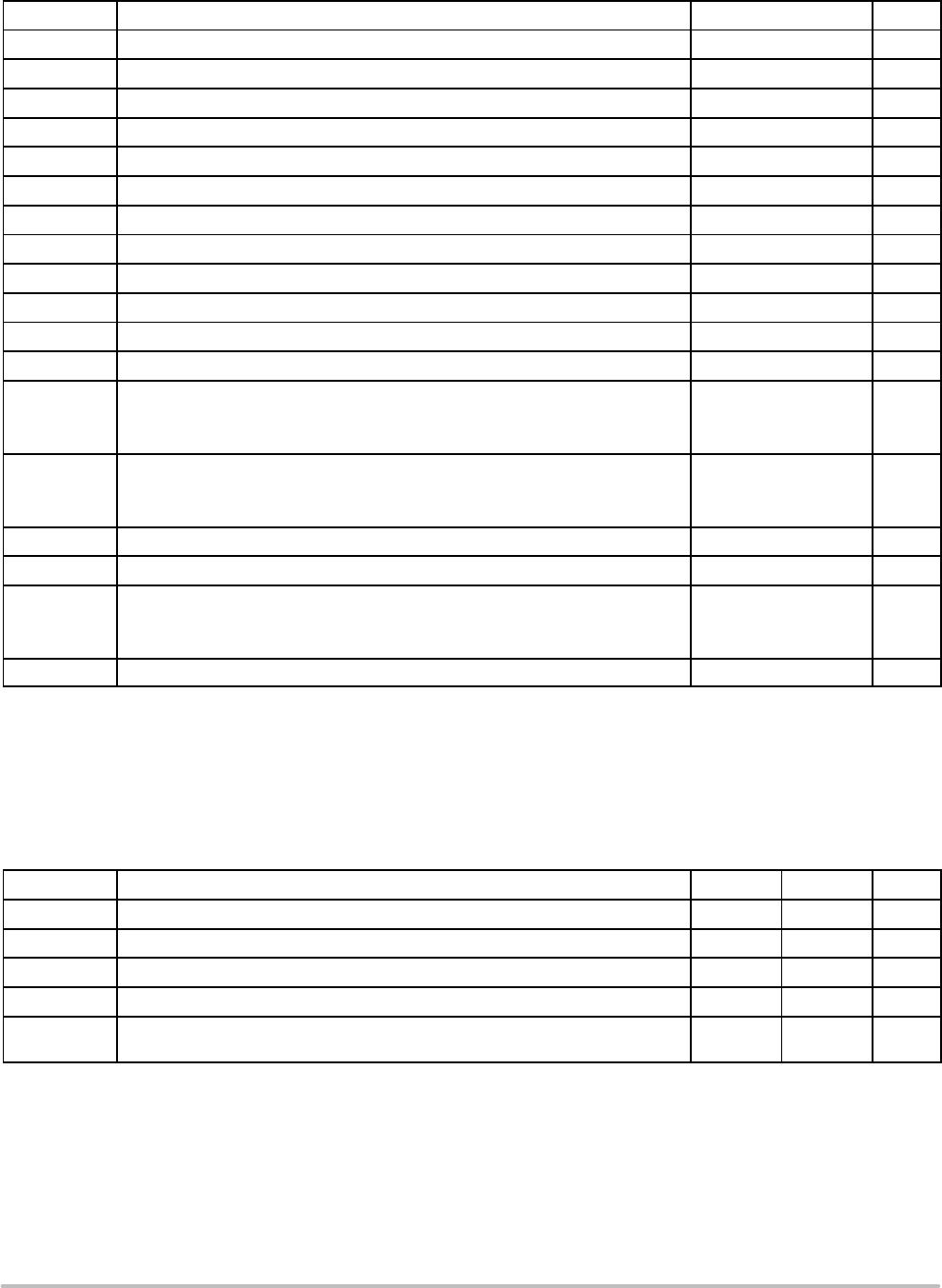
Table 1. MAXIMUM RATINGS
Symbol Parameter Value Unit
V
CC
DC Supply Voltage 0.5 to +7.0 V
V
IN
Control Pin Input Voltage 0.5 to +7.0 V
V
I/O
Switch Input / Output Voltage 0.5 to +7.0 V
I
IK
Control Pin DC Input Diode Current V
IN
< GND 50 mA
I
OK
Switch I/O Port DC Diode Current V
I/O
< GND 50 mA
I
O
OnState Switch Current ±128 mA
Continuous Current Through V
CC
or GND ±150 mA
I
CC
DC Supply Current per Supply Pin ±150 mA
I
GND
DC Ground Current per Ground Pin ±150 mA
T
STG
Storage Temperature Range 65 to +150 °C
T
L
Lead Temperature, 1 mm from Case for 10 Seconds 260 °C
T
J
Junction Temperature Under Bias 150 °C
q
JA
Thermal Resistance SC705/SC88A (Note 1)
TSOP5
ULLGA6/UDFN6
350
230
496
°C/W
P
D
Power Dissipation in Still Air at 85°C SC705/SC88A (Note 1)
TSOP5
ULLGA6/UDFN6
150
200
252
mW
MSL Moisture Sensitivity Level 1
F
R
Flammability Rating Oxygen Index: 28 to 34 UL 94 V0 @ 0.125 in
V
ESD
ESD Withstand Voltage Human Body Mode (Note 2)
Machine Mode (Note 3)
Charged Device Mode (Note 4)
>2000
>200
N/A
V
I
LATCHUP
Latchup Performance Above V
CC
and Below GND at 85°C (Note 5) ±100 mA
Stresses exceeding Maximum Ratings may damage the device. Maximum Ratings are stress ratings only. Functional operation above the
Recommended Operating Conditions is not implied. Extended exposure to stresses above the Recommended Operating Conditions may affect
device reliability.
1. Measured with minimum pad spacing on an FR4 board, using 10 mmby1 inch, 2 ounce copper trace no air flow.
2. Tested to EIA/ JESD22A114A
3. Tested to EIA/ JESD22A115A
4. Tested to JESD22C101A
5. Tested to EIA / JESD78.
Table 2. RECOMMENDED OPERATING CONDITIONS
Symbol Parameter Min Max Unit
V
CC
Positive DC Supply Voltage 4.0 5.5 V
V
I
Control Pin Input Voltage 0 5.5 V
V
I/O
Switch Input / Output Voltage 0 5.5 V
T
A
Operating FreeAir Temperature 55 +125 °C
Dt / DV
Input Transition Rise or Fall Rate Control Input
Switch I/O
0
0
5
DC
nS/V
7SB3126
http://onsemi.com
3
Table 3. DC ELECTRICAL CHARACTERISTICS
Symbol Parameter Conditions V
CC
(V)
T
A
= 255C T
A
= 555C to +1255C
Unit
Min Typ Max Min Max
V
IK
Clamp Diode Voltage I
IN
= 18 mA 4.5 1.2 1.2 V
V
IH
HighLevel Input Voltage
(Control)
4.0 to 5.5 2.0 2.0 V
V
IL
LowLevel Input Voltage
(Control)
4.0 to 5.5 0.8 0.8 V
I
IN
Input Leakage Current 0 V
IN
5.5 V 5.5 ±0.1 ±1.0
mA
I
OFF
Power Off Leakage Current V
I/O
= 0 to 5.5 V 0 ±0.1 ±1.0
mA
I
CC
Quiescent Supply Current I
O
= 0, V
IN
=
V
CC
or 0 V
5.5 ±0.1 ±1.0
mA
DI
CC
Increase in Supply Current
(Control Pin)
One input at 3.4
V; Other inputs
at V
CC
or GND
5.5 2.5 mA
R
ON
Switch ON Resistance
V
I/O
= 0,
I
I/O
= 64 mA
I
I/O
= 30 mA
4.5
3
3
7
7
7
7
W
V
I/O
= 2.4,
I
I/O
= 15 mA
4.5
6 15 15
V
I/O
= 2.4,
I
I/O
= 15 mA
4.0
10 20 20
Table 4. AC ELECTRICAL CHARACTERISTICS
Symbol Parameter V
CC
(V) Test Condition
T
A
= 255C
T
A
= 555C
to +1255C
Unit
Min Typ Max Min Max
t
PD
Propagation Delay,
A to B or B to A
4.0 to 5.5
See Figure 3
0.25 0.25
ns
0.25 0.25
t
EN
Output Enable Time
4.5 to 5.5 0.8 2.5 4.2 0.8 4.2
ns
4.0 0.8 3.0 4.6 0.8 4.6
t
DIS
Output Disable Time
4.5 to 5.5 0.8 3.1 4.8 0.8 4.8
ns
4.0 0.8 2.9 4.4 0.8 4.4
C
IN
Control Input Capacitance 5.0 V
IN
= 3 V or 0 2.0 pF
C
IO(ON)
Switch On Capacitance 5.0 Switch ON 10 pF
C
IO(OFF)
Switch Off Capacitance 5.0 Switch OFF 3.5 pF

7SB3126MUTCG

Mfr. #:
Manufacturer:
ON Semiconductor
Description:
Bus Transmitters 1 BIT BUS SWITCH INTEGRATED MO
Lifecycle:
New from this manufacturer.
Delivery:
DHL FedEx Ups TNT EMS
Payment:
T/T Paypal Visa MoneyGram Western Union