7SB3126MUTCG

7SB3126
http://onsemi.com
4
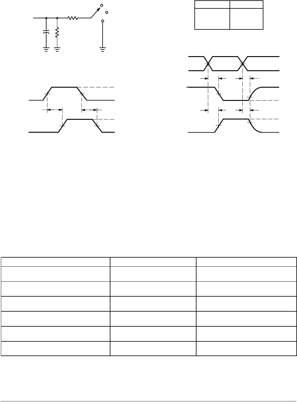
AC Loading and Waveforms
Figure 4. Load Circuit and Voltage Waveforms
500 W
C
L
= 50 pF
(see Note A)
7 V
From Output
Under Test
500 W
S1
Open
GND
LOAD CIRCUIT
TEST S1
t
PD
t
PLZ
/t
PZL
t
PHZ
/t
PZH
Open
7 V
GND
Input
1.5 V
1.5 V
1.5 V
1.5 V
t
PLH
t
PHL
Output
3 V
V
OH
0 V
V
OL
VOLTAGE WAVEFORMS
PROPAGATION DELAY TIMES
t
PZL
3 V
1.5 V
1.5 V
0 V
Output
Control
t
PLZ
t
PZH
t
PHZ
1.5 V
1.5 V
3.5 V
0 V
V
OL
V
OH
V
OL
+ 0.3 V
V
OH
0.3 V
Output
Waveform 1
S1 at 7 V
(see Note B)
Output
Waveform 2
S1 at Open
(see Note B)
VOLTAGE WAVEFORMS
ENABLE AND DISABLE TIMES
A. C
L
includes probe and jig capacitance.
B. Waveform 1 is for an output with internal conditions such that the output is low, except when disabled by the output control.
Waveform 2 is for an output with internal conditions such that the output is high, except when disabled by the output control.
C. All input pulses are supplied by generators having the following characteristics: PRR 10 MHz, Z
O
= 50 W, t
r
2.5 ns, t
f
2.5 ns.
D. The output is measured with one input transition per measurement.
E. t
PLZ
and t
PHZ
are the same as t
dis
.
F. t
PZL
and t
PZH
are the same as t
en
.
G. t
PLH
and t
PHL
are the same as t
pd
.
DEVICE ORDERING INFORMATION
Device Package Shipping
7SB3126DTT1G TSOP5
(PbFree)
3000 / Tape & Reel
7SB3126DFT2G SC88A
(PbFree)
3000 / Tape & Reel
7SB3126AMX1TCG ULLGA6 0.5 mm Pitch
(PbFree)
3000 / Tape & Reel
7SB3126BMX1TCG ULLGA6 0.4 mm Pitch
(PbFree)
3000 / Tape & Reel
7SB3126CMX1TCG ULLGA6 0.35 mm Pitch
(PbFree)
3000 / Tape & Reel
7SB3126MUTCG UDFN6 0.4 mm Pitch
(PbFree)
3000 / Tape & Reel
For information on tape and reel specifications, including part orientation and tape sizes, please refer to our Tape and Reel Packaging
Specifications Brochure, BRD8011/D.
7SB3126
http://onsemi.com
5
PACKAGE DIMENSIONS
NOTES:
1. DIMENSIONING AND TOLERANCING
PER ANSI Y14.5M, 1982.
2. CONTROLLING DIMENSION: INCH.
3. 419A01 OBSOLETE. NEW STANDARD
419A02.
4. DIMENSIONS A AND B DO NOT INCLUDE
MOLD FLASH, PROTRUSIONS, OR GATE
BURRS.
DIM
A
MIN MAX MIN MAX
MILLIMETERS
1.80 2.200.071 0.087
INCHES
B 1.15 1.350.045 0.053
C 0.80 1.100.031 0.043
D 0.10 0.300.004 0.012
G 0.65 BSC0.026 BSC
H --- 0.10---0.004
J 0.10 0.250.004 0.010
K 0.10 0.300.004 0.012
N 0.20 REF0.008 REF
S 2.00 2.200.079 0.087
B0.2 (0.008)
MM
12 3
45
A
G
S
D
5 PL
H
C
N
J
K
B
SC88A, SOT353, SC70
CASE 419A02
ISSUE J
7SB3126
http://onsemi.com
6
PACKAGE DIMENSIONS
TSOP5
CASE 48302
ISSUE H
NOTES:
1. DIMENSIONING AND TOLERANCING PER
ASME Y14.5M, 1994.
2. CONTROLLING DIMENSION: MILLIMETERS.
3. MAXIMUM LEAD THICKNESS INCLUDES
LEAD FINISH THICKNESS. MINIMUM LEAD
THICKNESS IS THE MINIMUM THICKNESS
OF BASE MATERIAL.
4. DIMENSIONS A AND B DO NOT INCLUDE
MOLD FLASH, PROTRUSIONS, OR GATE
BURRS.
5. OPTIONAL CONSTRUCTION: AN
ADDITIONAL TRIMMED LEAD IS ALLOWED
IN THIS LOCATION. TRIMMED LEAD NOT TO
EXTEND MORE THAN 0.2 FROM BODY.
DIM MIN MAX
MILLIMETERS
A 3.00 BSC
B 1.50 BSC
C 0.90 1.10
D 0.25 0.50
G 0.95 BSC
H 0.01 0.10
J 0.10 0.26
K 0.20 0.60
L 1.25 1.55
M 0 10
S 2.50 3.00
123
54
S
A
G
L
B
D
H
C
J
__
0.7
0.028
1.0
0.039
ǒ
mm
inches
Ǔ
SCALE 10:1
0.95
0.037
2.4
0.094
1.9
0.074
*For additional information on our PbFree strategy and soldering
details, please download the ON Semiconductor Soldering and
Mounting Techniques Reference Manual, SOLDERRM/D.
SOLDERING FOOTPRINT*
0.20
5X
C AB
T0.10
2X
2X
T0.20
NOTE 5
T
SEATING
PLANE
0.05
K
M
DETAIL Z
DETAIL Z

7SB3126MUTCG

Mfr. #:
Manufacturer:
ON Semiconductor
Description:
Bus Transmitters 1 BIT BUS SWITCH INTEGRATED MO
Lifecycle:
New from this manufacturer.
Delivery:
DHL FedEx Ups TNT EMS
Payment:
T/T Paypal Visa MoneyGram Western Union