High current connectors B01
–2–
ACCTB71E 201602-T
PRODUCT TYPES
Notes: 1. Order unit:
For volume production: 1-inner carton (1-reel) units
For samples, please contact our sales office.
2. Please contact us for connectors having a number of pins other than those listed above.
SPECIFICATIONS
1. Characteristics
2. Material and surface treatment
Stacking height Number of contacts
Part number Packing
Socket Header Inner carton (1-reel) Outer carton
0.6mm 6 AXF361500 AXF461500 15,000 pieces 30,000 pieces
0.8mm 6 AXF363500 AXF463500 15,000 pieces 30,000 pieces
Item Specifications Conditions
Electrical
characteristics
Rated current
3.0 A/pin contact (Power terminal)
0.3 A/pin contact (Signal terminal)
Rated voltage 30V AC/DC
Insulation resistance Min. 1,000MΩ (Initial stage) Using 250V DC megger (applied for 1 minute)
Dielectric strength 150V AC for 1 minute
No short-circuiting or damage at a detection current of 1 mA
when the specified voltage is applied for one minute.
Contact resistance
Power terminal: Max. 20mΩ
Signal terminal: Max. 90mΩ
According to the contact resistance measurement method of
JIS C 5402
Mechanical
characteristics
Composite insertion force Max. 40 N
Composite removal force Min. 10 N (H: 0.6, Initial stage)
Environmental
characteristics
Ambient temperature –55°C to +85°C No icing or condensation.
Storage temperature
–55°C to +85°C (Products only)
–40°C to +50°C (Packaging structure)
No icing or condensation.
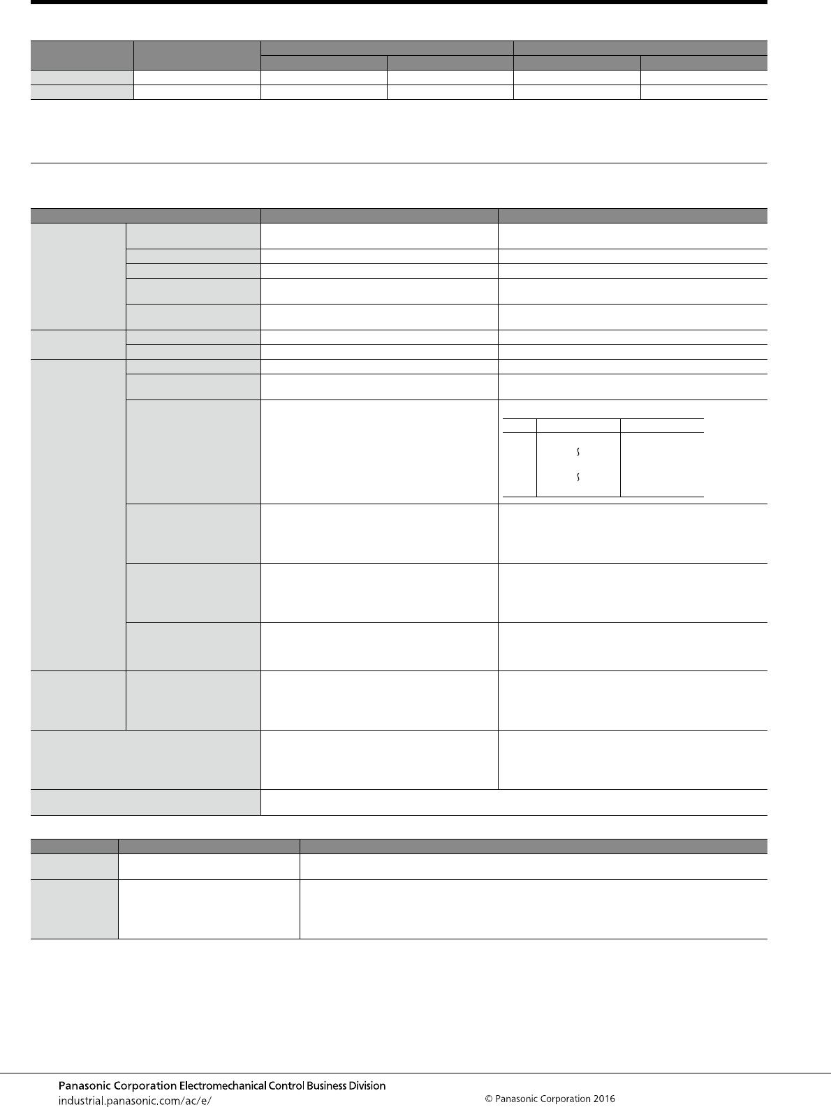
Thermal shock resistance
(Header and socket mated)
After 5 cycles
Insulation resistance: Min. 100MΩ,
Contact resistance
Power terminal: Max. 20mΩ
Signal terminal: Max. 90mΩ
Conformed to MIL-STD-202F, method 107G
Humidity resistance
(Header and socket mated)
After 120 hours
Insulation resistance: Min. 100MΩ,
Contact resistance
Power terminal: Max. 20mΩ
Signal terminal: Max. 90mΩ
Conformed to IEC60068-2-78
Bath temperature 40°C±2°C,
Humidity 90% to 95% R.H.
Salt water spray resistance
(Header and socket mated)
After 24 hours
Insulation resistance: Min. 100MΩ,
Contact resistance
Power terminal: Max. 20mΩ
Signal terminal: Max. 90mΩ
Conformed to IEC60068-2-11
Bath temperature 35°C±2°C,
Salt water concentration 5%±1%
H2S resistance
(Header and socket mated)
After 48 hours
Contact resistance
Power terminal: Max. 20mΩ
Signal terminal: Max. 90mΩ
Conformed to JEIDA-38-1984
Bath temperature 40°C±2°C,
Gas concentration 3 ppm ±1 ppm,
Humidity 75% to 80% R.H.
Lifetime
characteristics
Insertion and removal life
Mechanical life: 30 times
Contact resistance:
Power terminal: Max. 20mΩ
Signal terminal: Max. 90mΩ
Composite removal force: Min. 7 N
Repeated insertion and removal cycles of max. 200 times/
hour
Soldering heat resistance
The initial specification must be satisfied electrically
and mechanically
Infrared reflow soldering: Max. peak temperature of 260°C
(PC board surface temperature near connector terminals)
Soldering iron:
300°C within 5 sec.
350°C within 3 sec.
Unit weight
6 pin contact Socket h = 0.6 mm: 0.010 g h = 0.8 mm: 0.013 g
Header h = 0.6 mm: 0.004 g h = 0.8 mm: 0.005 g
Part name Material Surface treatment
Molded portion
Heat resistant plastic (LCP resin)
(UL94V-0)
—
Contact and Post Copper alloy
Contact portion (Main): Au plating (Min. 0.1μm) over nickel
Contact portion (Sub): Au plating (Min. 0. 05μm) over nickel
Terminal portion: Au plating over nickel (except for top of the terminal)
Soldering terminals (Socket): Pd + Au flash plating over nickel (except for top of the terminal)
Soldering terminals (Header): Au plating over nickel (except for top of the terminal)
Order Temperature (°C) Time (minutes)
1
2
3
4
–55
85
–55
0
−3
30
Max. 5
30
Max. 5
+3
0
0
−3

