ADVFC32BH

REV. B
Information furnished by Analog Devices is believed to be accurate and
reliable. However, no responsibility is assumed by Analog Devices for its
use, nor for any infringements of patents or other rights of third parties
which may result from its use. No license is granted by implication or
otherwise under any patent or patent rights of Analog Devices.
a
ADVFC32
One Technology Way, P.O. Box 9106, Norwood, MA 02062-9106, U.S.A.
Tel: 781/329-4700 World Wide Web Site: http://www.analog.com
Fax: 781/326-8703 © Analog Devices, Inc., 2000
Voltage-to-Frequency and
Frequency-to-Voltage Converter
FEATURES
High Linearity
0.01% Max at 10 kHz FS
0.05% Max at 100 kHz FS
0.2% Max at 500 kHz FS
Output TTL/CMOS-Compatible
V/F or F/V Conversion
6 Decade Dynamic Range
Voltage or Current Input
Reliable Monolithic Construction
MIL-STD-883-Compliant Versions Available
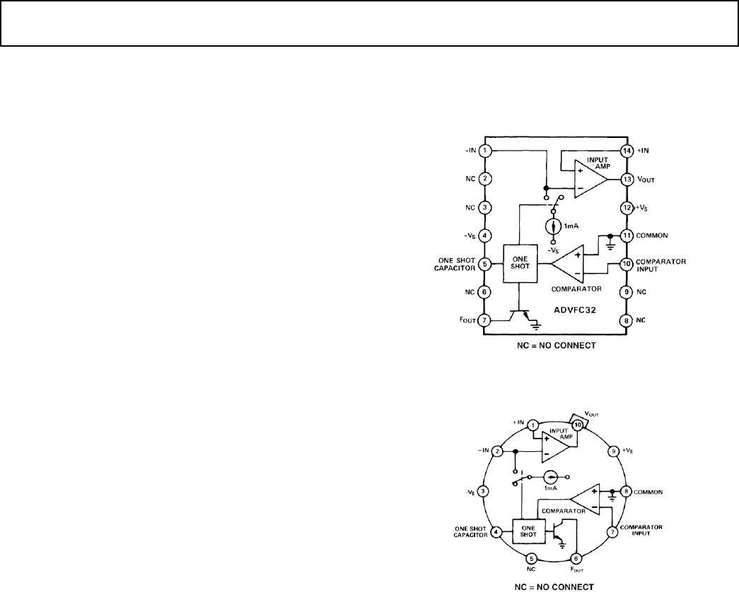
PIN CONFIGURATION
(TOP VIEW)
N-14 Package
H-10A Package
PRODUCT DESCRIPTION
The industry standard ADVFC32 is a low cost monolithic
voltage-to-frequency (V/F) converter or frequency-to-voltage
(F/V) converter with good linearity (0.01% max error at 10 kHz)
and operating frequency up to 0.5 MHz. In the V/F configuration,
positive or negative input voltages or currents can be converted
to a proportional frequency using only a few external compo-
nents. For F/V conversion, the same components are used with
a simple biasing network to accommodate a wide range of input
logic levels.
TTL or CMOS compatibility is achieved in the V/F operating
mode using an open collector frequency output. The pull-up
resistor can be connected to voltages up to 30 volts, or to 15 V
or 5 V for conventional CMOS or TTL logic levels. This resis-
tor should be chosen to limit current through the open collector
output to 8 mA. A larger resistance can be used if driving a high
impedance load.
Input offset drift is only 3 ppm of full scale per °C, and full-
scale calibration drift is held to a maximum of 100 ppm/°C
(ADVFC32BH) due to a low T.C. Zener diode.
The ADVFC32 is available in commercial, industrial, and
extended temperature grades. The commercial grade is pack-
aged in a 14-lead plastic DIP while the two wider temperature
range parts are packaged in hermetically sealed 10-lead cans.
PRODUCT HIGHLIGHTS
1. The ADVFC32 uses a charge balancing circuit technique
(see Functional Block Diagram) which is well suited to high
accuracy voltage-to-frequency conversion. The full-scale
operating frequency is determined by only one precision
resistor and capacitor. The tolerance of other support compo-
nents (including the integration capacitor) is not critical.
Inexpensive ±20% resistors and capacitors can be used with-
out affecting linearity or temperature drift.
2. The ADVFC32 is easily configured to satisfy a wide range of
system requirements. Input voltage scaling is set by selecting
the input resistor which sets the input current to 0.25 mA at
the maximum input voltage.
3. The same components used for V/F conversion can also be
used for F/V conversion by adding a simple logic biasing
network and reconfiguring the ADVFC32.
4. The ADVFC32 is intended as a pin-for-pin replacement for
VFC32 devices from other manufacturers.
5. The ADVFC32 is available in versions compliant with MIL-
STD-883. Refer to the Analog Devices Military Products
Databook or current ADVFC32/883B data sheet for detailed
specifications.
ADVFC32* PRODUCT PAGE QUICK LINKS
Last Content Update: 02/23/2017
COMPARABLE PARTS
View a parametric search of comparable parts.
DOCUMENTATION
Application Notes
AN-276: Analog to Digital Conversion by Using V/F
Converters
Data Sheet
ADVFC32: Low Cost Monolithic V/F Converter or F/V
Converter Data Sheet
DESIGN RESOURCES
ADVFC32 Material Declaration
PCN-PDN Information
Quality And Reliability
Symbols and Footprints
DISCUSSIONS
View all ADVFC32 EngineerZone Discussions.
SAMPLE AND BUY
Visit the product page to see pricing options.
TECHNICAL SUPPORT
Submit a technical question or find your regional support
number.
DOCUMENT FEEDBACK
Submit feedback for this data sheet.
This page is dynamically generated by Analog Devices, Inc., and inserted into this data sheet. A dynamic change to the content on this page will not
trigger a change to either the revision number or the content of the product data sheet. This dynamic page may be frequently modified.
REV. B
–2–
ADVFC32–SPECIFICATIONS
(typical @ 25C with V
S
= 15 V unless otherwise noted.)
ADVFC32K ADVFC32B ADVFC32S
Model Min Typ Max Min Typ Max Min Typ Max Unit
DYNAMIC PERFORMANCE
Full-Scale Frequency Range 0 500 0 500 0 500 kHz
Nonlinearity
1
f
MAX
= 10 kHz –0.01 ±0.01 –0.01 +0.01 –0.01 +0.01 %
f
MAX
= 100 kHz –0.05 +0.05 –0.05 +0.05 –0.05 +0.05 %
f
MAX
= 0.5 MHz –0.20 ±0.05 +0.20 –0.20 ±0.05 +0.20 –0.20 ±0.05 +0.20 %
Full-Scale Calibration Error
(Adjustable to Zero) ±5 ±5 ±5%
vs. Supply
(Full-Scale Frequency = 100 kHz)
–0.015 +0.015 –0.015 +0.015 –0.015 +0.015
% of FSR%
vs. Temperature
(Full-Scale Frequency = 10 kHz)
±75 –100 +100 +150 +150
ppm/°C
DYNAMIC RESPONSE
Maximum Settling Time for Full Scale
Step Input 1 Pulse of New Frequency Plus 1 µs 1 Pulse of New Frequency Plus 1 µs 1 Pulse of New Frequency Plus 1 µs
Overload Recovery Time 1 Pulse of New Frequency Plus 1 µs 1 Pulse of New Frequency Plus 1 µs 1 Pulse of New Frequency Plus 1 µs
ANALOG INPUT AMPLIFIER
(V/F Conversion)
Current Input Range 0 0.25 0 0.25 0 0.25 mA
Voltage Input Range 0 –10 0 –10 0 –10 V
2
0.25 0.25 0.25 mA
× R
IN
3
× R
IN
3
× R
IN
3
Differential Impedance
300 kΩ||10 pF
2 MΩ||10 pF 300 kΩ||10 pF 2 MΩ||10 pF 300 kΩ||10 pF 2 MΩ||10 pF
Common-Mode Impedance 300 MΩ||3 pF 750 MΩ||3 pF 300 MΩ||3 pF 750 MΩ||10 pF 300 MΩ||3 pF 750 MΩ||10 pF
Input Bias Current
Noninverting Input 40 250 40 250 40 250 nA
Inverting Input –100 ±8 +100 –100 ±8 +100 –100 ±8 +100 nA
Input Offset Voltage
(Trimmable to Zero)
2, 3
444mV
vs. Temperature (T
MIN
to T
MAX
)30 30 30 µV/°C
Safe Input Voltage ±V
S
±V
S
±V
S
COMPARATOR (F/V Conversion)
Logic “0” Level –V
S
–0.6 –V
S
–0.6 –V
S
–0.6 V
Logic “1” Level 1 +V
S
1+V
S
1+V
S
V
Pulse Width Range
4
0.1 0.15/f
MAX
0.1 0.15/f
MAX
0.1
0.15/f
MAX
µs
Input Impedance 50 kΩ||10 pF 250 k 50 kΩ||10 pF 250 k 50 kΩ||10 pF 250 k
OPEN COLLECTOR OUTPUT
(V/F Conversion)
Output Voltage in Logic “0”
I
SINK
= 8 mA 0.4 0.4 0.4 V
Output Leakage Current in Logic “1”
111µA
Voltage Range 0 30 0 30 0 30 V
Fall Times (Load = 500 pF and
I
SINK
= 5 mA) 400 400 400 ns
AMPLIFIER OUTPUT (F/V Conversion)
Voltage Range (0 mAI
O
7 mA) 0 10 0 10 0 10 V
Source Current (0V
O
7 V) 10 10 10 mA
Capacitive Load (Without Oscillation) 100 100 100 pF
Closed Loop Output Impedance 1 1 1
POWER SUPPLY
Rated Voltage ±15 ± 15 ±15 V
Voltage Range ±9 ±18 ±9 ±18 ±9 ±18 V
Quiescent Current 6 8 6 8 6 8 mA
TEMPERATURE RANGE
Specified Range 0 +70 –25 +85 –55 +125 °C
Operating Range –25 +85 –55 +125 –55 +125 °C
Storage –25 +85 –65 +150 –65 +150 °C
PACKAGE OPTIONS
Plastic DIP (N-14) ADVFC32KN
TO–100 (H-10A)
ADVFC32BH ADVFC32SH
NOTES
1
Nonlinearity defined as deviation from a straight line from zero to full scale, expressed as a percentage of full scale.
2
See Figure 3.
3
See Figure 1.
4
f
MAX
expressed in units of MHz.
Specifications shown in boldface are tested on all production units at final electrical test. Results from those tests are used to calculate outgoing quality levels. All min and max specifications are
guaranteed, although only those shown in boldface are tested on all production units.
Specifications subject to change without notice.

ADVFC32BH

Mfr. #:
Manufacturer:
Analog Devices Inc.
Description:
Voltage to Frequency & Frequency to Voltage V/F Converter IC
Lifecycle:
New from this manufacturer.
Delivery:
DHL FedEx Ups TNT EMS
Payment:
T/T Paypal Visa MoneyGram Western Union

Products related to this Datasheet