REV. B
–6–
C00443c–0–11/00 (rev. B)
PRINTED IN U.S.A.
ADVFC32
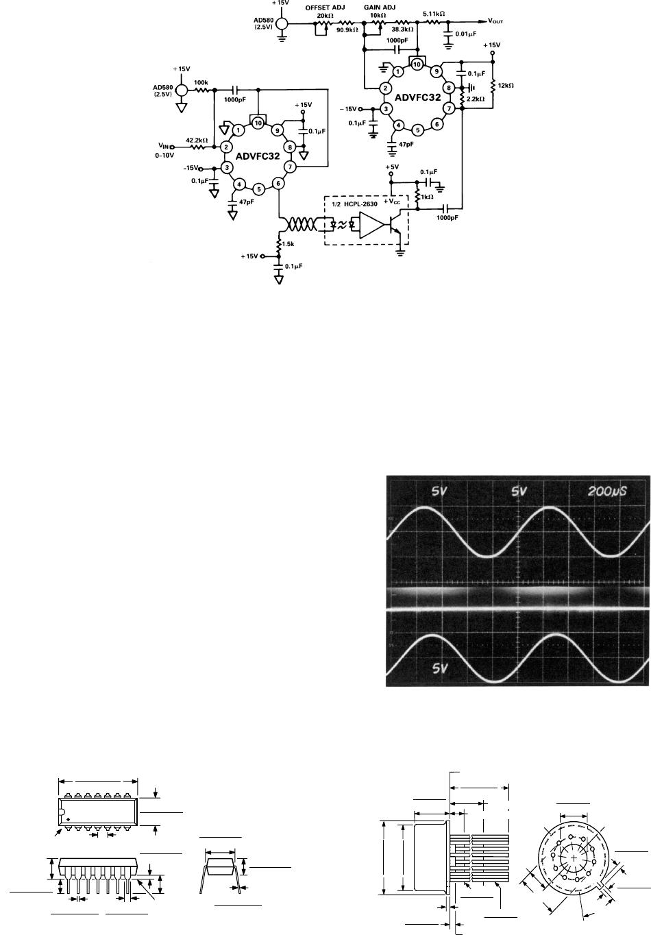
Figure 6. High Noise Immunity Data Link
OUTLINE DIMENSIONS
Dimensions shown in inches and (mm).
14-Lead Plastic DIP (N-14)
14
17
8
PIN 1
0.795 (20.19)
0.725 (18.42)
0.280 (7.11)
0.240 (6.10)
0.100 (2.54)
BSC
SEATING
PLANE
0.060 (1.52)
0.015 (0.38)
0.210 (5.33)
MAX
0.022 (0.558)
0.014 (0.356)
0.160 (4.06)
0.115 (2.93)
0.070 (1.77)
0.045 (1.15)
0.130
(3.30)
MIN
0.195 (4.95)
0.115 (2.93)
0.015 (0.381)
0.008 (0.204)
0.325 (8.25)
0.300 (7.62)
TO-100 (H-10A)
0.250 (6.35) MIN
0.750 (19.05)
0.500 (12.70)
0.185 (4.70)
0.165 (4.19)
REFERENCE PLANE
0.050 (1.27) MAX
0.019 (0.48)
0.016 (0.41)
0.021 (0.53)
0.016 (0.41)
0.045 (1.14)
0.010 (0.25)
0.040 (1.02) MAX
BASE & SEATING PLANE
0.335 (8.51)
0.305 (7.75)
0.370 (9.40)
0.335 (8.51)
1
0.034 (0.86)
0.027 (0.69)
0.045 (1.14)
0.027 (0.69)
0.160 (4.06)
0.110 (2.79)
6
2
8
7
5
4
3
0.115
(2.92)
BSC
9
10
0.230 (5.84)
BSC
36° BSC
The data link input voltage is changed in a frequency modulated
signal by the first ADVFC32. A 42.2 kΩ input resistor and a
100 kΩ offset resistor set the scaling so that a 0 V input signal
corresponds to 50 kHz, and a 10 V input results in the maximum
output frequency of 500 kHz. A high frequency optocoupler is
then used to transmit the signal across any common-mode volt-
age potentials to the receiving ADVFC32. The optocoupler is
not necessary in systems where common-mode noise is either
very small or a constant low level dc voltage. In systems where
common-mode voltage may present a problem, the connection
between the two locations should be through the optocoupler;
no power or ground connections need to be made.
The output of the optocoupler drives an ADVFC32 hooked up
in the F/V configuration. Since the reconstructed signal at Pin
10 has a considerable amount of carrier feedthrough, it is desir-
able to filter out any frequencies in the carrier range of 50 kHz
to 500 kHz. The frequency response of the F/V converter is only
3 kHz due to the pole made by the integrator, so a second 3 kHz
filter will not significantly limit the bandwidth. With the simple
one pole filter shown in Figure 6, the input to output 3 dB point
is approximately 2 kHz, and the output noise is less than 15 mV.
If a lower output impedance drive is needed, a two-pole active
filter is recommended as an output stage.
Although the F/V conversion technique used in this circuit is
quite simple, it is also very limited in terms of its frequency
response and output ripple. The frequency response is limited
by the integrator time constant and while it is possible to decrease
that time constant, either signal range or output ripple must be
sacrificed. The performance of the circuit of Figure 6 is shown
in the photograph below. The top trace is the input signal, the
middle trace is the frequency-modulated signal at the opto-
coupler’s output, and the bottom trace is the recovered signal at
the output of the F/V converter.