IRF9Z20, SiHF9Z20
www.vishay.com
Vishay Siliconix
S16-0015-Rev. C, 18-Jan-16
1
Document Number: 90121
For technical questions, contact: hvm@vishay.com
THIS DOCUMENT IS SUBJECT TO CHANGE WITHOUT NOTICE. THE PRODUCTS DESCRIBED HEREIN AND THIS DOCUMENT
ARE SUBJECT TO SPECIFIC DISCLAIMERS, SET FORTH AT www.vishay.com/doc?91000
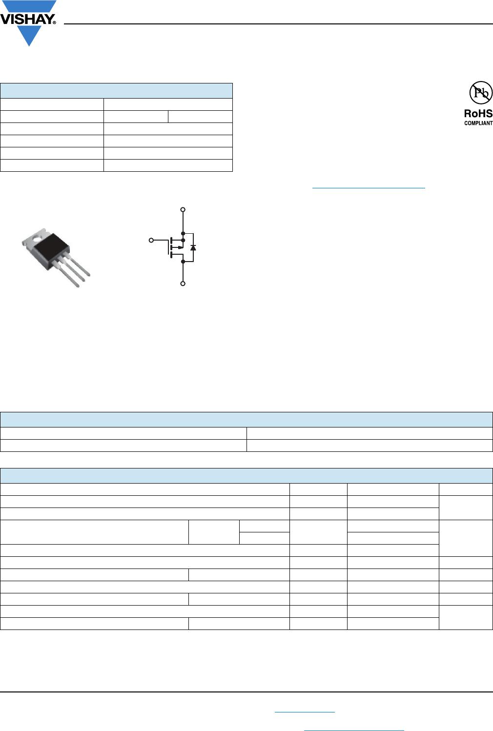
Power MOSFET
FEATURES
• P-channel versatility
• Compact plastic package
•Fast switching
• Low drive current
• Ease of paralleling
• Excellent temperature stability
• Material categorization: for definitions of compliance
please see www.vishay.com/doc?99912
DESCRIPTION
The power MOSFET technology is the key to Vishay’s
advanced line of power MOSFET transistors. The efficient
geometry and unique processing of the power MOSFET
design achieve very low on-state resistance combined with
high transconductance and extreme device ruggedness.
The P-channel power MOSFETs are designed for
application which require the convenience of reverse
polarity operation. They retain all of the features of the more
common N-channel power MOSFETs such as voltage
control, very fast switching, ease of paralleling, and
excellent temperature stability.
P-channel power MOSFETs are intended for use in power
stages where complementary symmetry with N-channel
devices offers circuit simplification. They are also very useful
in drive stages because of the circuit versatility offered by
the reverse polarity connection. Applications include motor
control, audio amplifiers, switched mode converters, control
circuits and pulse amplifiers.
Notes
a. Repetitive rating; pulse width limited by maximum junction temperature (see fig. 14).
b. V
DD
= - 25 V, starting T
J
= 25 °C, L =100 μH, R
g
= 25
c. 0.063" (1.6 mm) from case.
PRODUCT SUMMARY
V
DS
(V) -50
R
DS(on)
()V
GS
= -10 V 0.28
Q
g
max. (nC) 26
Q
gs
(nC) 6.2
Q
gd
(nC) 8.6
Configuration Single
S
G
D
P-Channel MOSFET
ORDERING INFORMATION
Package TO-220AB
Lead (Pb)-free IRF9Z20PbF
ABSOLUTE MAXIMUM RATINGS (T
C
= 25 °C, unless otherwise noted)
PARAMETER SYMBOL LIMIT UNIT
Drain-Source Voltage V
DS
-50
V
Gate-Source Voltage V
GS
± 20
Continuous Drain Current V
GS
at - 10 V
T
C
= 25 °C
I
D
-9.7
AT
C
= 100 °C -6.1
Pulsed Drain Current
a
I
DM
-39
Linear Derating Factor 0.32 W/°C
Inductive Current, Clamped L = 100 μH I
LM
-39 A
Unclamped Inductive Current (Avalanche current) I
L
-2.2 A
Maximum Power Dissipation T
C
= 25 °C P
D
40 W
Operating Junction and Storage Temperature Range T
J
, T
stg
-55 to +150
°C
Soldering Recommendations (Peak temperature)
c
for 10 s 300