IRF9Z20PBF

IRF9Z20, SiHF9Z20
www.vishay.com
Vishay Siliconix
S16-0015-Rev. C, 18-Jan-16
4
Document Number: 90121
For technical questions, contact: hvm@vishay.com
THIS DOCUMENT IS SUBJECT TO CHANGE WITHOUT NOTICE. THE PRODUCTS DESCRIBED HEREIN AND THIS DOCUMENT
ARE SUBJECT TO SPECIFIC DISCLAIMERS, SET FORTH AT www.vishay.com/doc?91000
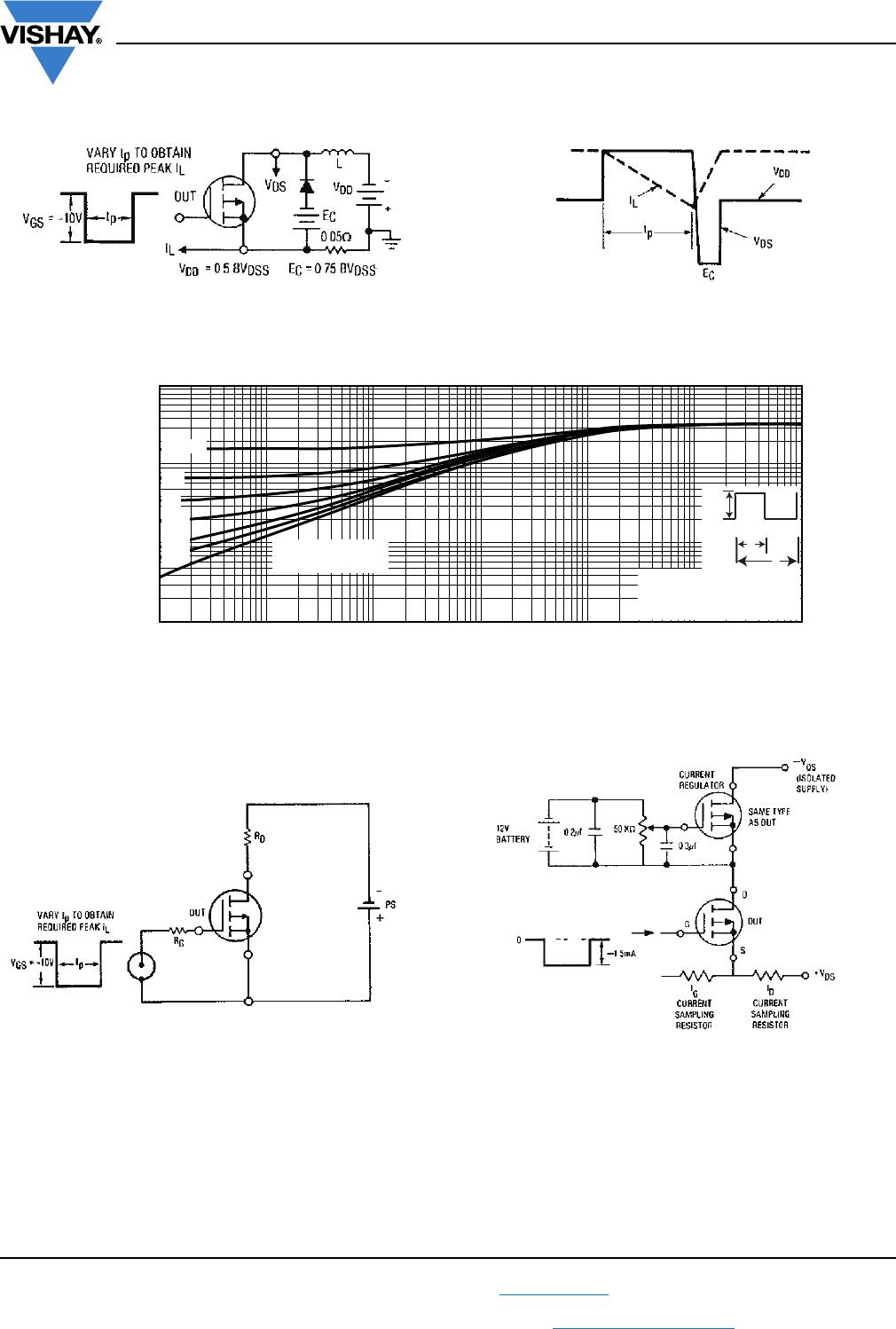
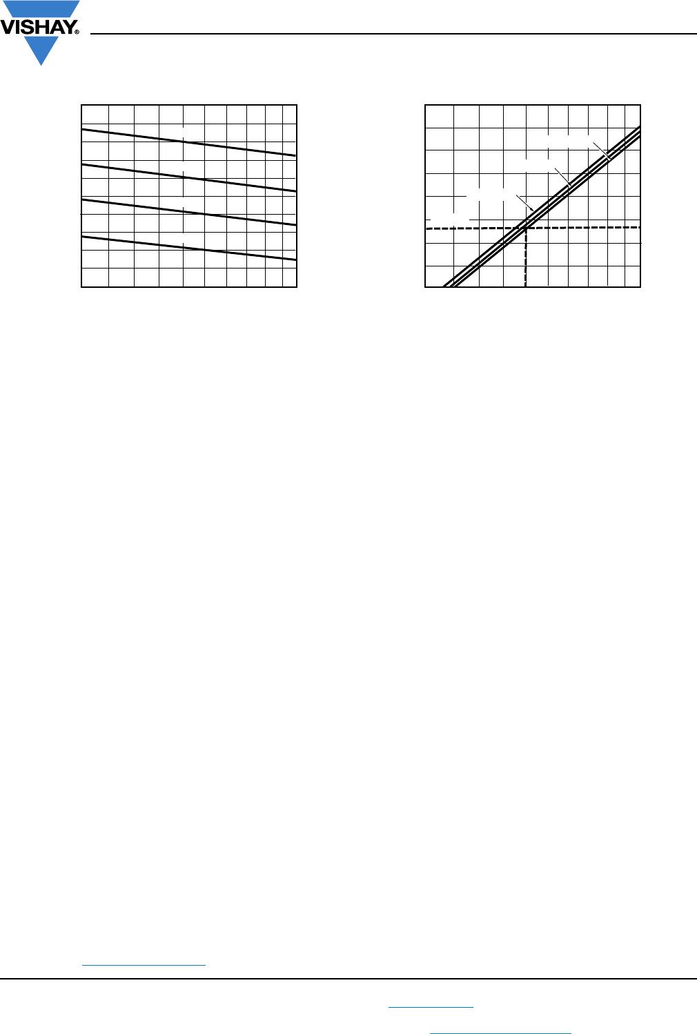
Fig. 7 - Breakdown Voltage vs. Temperature
Fig. 8 - Normalized On-Resistance vs. Temperature
Fig. 9 - Typical Capacitance vs. Drain-to-Source Voltage
Fig. 10 - Typical Gate Charge vs. Gate-to-Source Voltage
Fig. 11 - Typical On-Resistance vs. Drain Current
Fig. 12 - Maximum Drain Current vs. Case Temperature
90121_08
T
J
, Junction Temperature (°C)
BV
DSS
, Drain-to-Source Breakdown
1.25
Voltage (Normalized)
1.15
0.75
0.85
0.95
1.05
- 60 - 40 - 20 0 20 40 60 80 100
120
140 160
I
D
= 1 mA
90121_09
T
J
, Junction Temperature (°C)
R
DS(on)
, Drain-to-Source On Resistance
3.0
(Normalized)
2.4
0.0
0.6
1.2
1.8
- 60 - 40 - 20 0 20 40 60 80 100 120 140 160
I
D
= - 9.7 A
V
GS
= - 10 V
1000
800
600
400
0
200
110
C, Capacitance (pF)
Negative V
DS
,
Drain-to-Source Voltage (V)
C
iss
C
rss
C
oss
90121_10
V
GS
= 0 V, f = 1 MHz
C
iss
= C
gs
+ C
gd
, C
ds
Shorted
C
rss
= C
gd
C
oss
= C
ds
+ C
gs
C
gd
/ (C
gs
+ C
gd
)
C
ds
+ C
gd
10
2
5252
Q
G
, Total Gate Charge (nC)
Negative V
GS
, Gate-to-Source Voltage (V)
20
16
12
8
0
4
0
8
40
3224
16
V
SD
= - 40 V
For test circuit
see figure 17
90121_11
I
D
= - 9.7 A
150
Negative I
D
, Drain Current (A)
T
C
, Case Temperature (°C)
2
4
6
8
10
25
90121_13
1251007550
0
IRF9Z20, SiHF9Z20
IRF9Z22, SiHF9Z22
IRF9Z20, SiHF9Z20
www.vishay.com
Vishay Siliconix
S16-0015-Rev. C, 18-Jan-16
5
Document Number: 90121
For technical questions, contact: hvm@vishay.com
THIS DOCUMENT IS SUBJECT TO CHANGE WITHOUT NOTICE. THE PRODUCTS DESCRIBED HEREIN AND THIS DOCUMENT
ARE SUBJECT TO SPECIFIC DISCLAIMERS, SET FORTH AT www.vishay.com/doc?91000
Fig. 13a - Unclamped Inductive Test Circuit Fig. 13b - Unclamped Inductive Load Test Waveforms
Fig. 14 - Maximum Effective Transient Thermal Impedance, Junction-to-Case vs. Pulse Duration
Fig. 15 - Switching Time Test Circuit Fig. 16 - Gate Charge Test Circuit
10
1
0.1
10
-2
10
-5
10
-4
10
-3
10
-2
0.1 1 10
P
DM
t
1
t
2
t
1
, Rectangular Pulse Duration (s)
Thermal Response (Z
thJC
)
Notes:
1. Duty Factor, D = t
1
/t
2
2. Peak T
j
= P
DM
x Z
thJC
+ T
C
Single Pulse
(Thermal Response)
D = 0.5
0.2
0.05
0.02
0.01
90121_05
0.1
IRF9Z20, SiHF9Z20
www.vishay.com
Vishay Siliconix
S16-0015-Rev. C, 18-Jan-16
6
Document Number: 90121
For technical questions, contact: hvm@vishay.com
THIS DOCUMENT IS SUBJECT TO CHANGE WITHOUT NOTICE. THE PRODUCTS DESCRIBED HEREIN AND THIS DOCUMENT
ARE SUBJECT TO SPECIFIC DISCLAIMERS, SET FORTH AT www.vishay.com/doc?91000
Fig. 17 - Typical Time to Accumulated 1 % Gate Failure Fig. 18 - Typical High Temperature Reverse Bias (HTRB)
Failure Rate
Vishay Siliconix maintains worldwide manufacturing capability. Products may be manufactured at one of several qualified locations. Reliability data for Silicon
Technology and Package Reliability represent a composite of all qualified locations. For related documents such as package/tape drawings, part marking, and
reliability data, see www.vishay.com/ppg?90121
.
90121_18
14 V
Time (H)
50
10
12
10
10
10
8
10
6
10
4
10
2
20 V
18 V
16 V
70 90
110
130
150
Temperature (°C)
90121_19
Random Failure Rate (FIT)
50
10
4
10
3
10
2
10
1
70 90
110
130
150
Temperature (°C)
% Per 1000 Hours
10
-4
10
-3
10
-2
0.1
1
60 % UCL
90 % UCL
99 % UCL
20 FIT’s

IRF9Z20PBF

Mfr. #:
Manufacturer:
Vishay / Siliconix
Description:
MOSFET P-Chan 50V 9.7 Amp
Lifecycle:
New from this manufacturer.
Delivery:
DHL FedEx Ups TNT EMS
Payment:
T/T Paypal Visa MoneyGram Western Union

Products related to this Datasheet