© Semiconductor Components Industries, LLC, 2014
April, 2014 − Rev. 1
1 Publication Order Number:
NSIC2020JB/D
NSIC2020JBT3G
Constant Current Regulator
& LED Driver for A/C off-line
Applications
120 V, 20 mA + 15%, 3 W Package
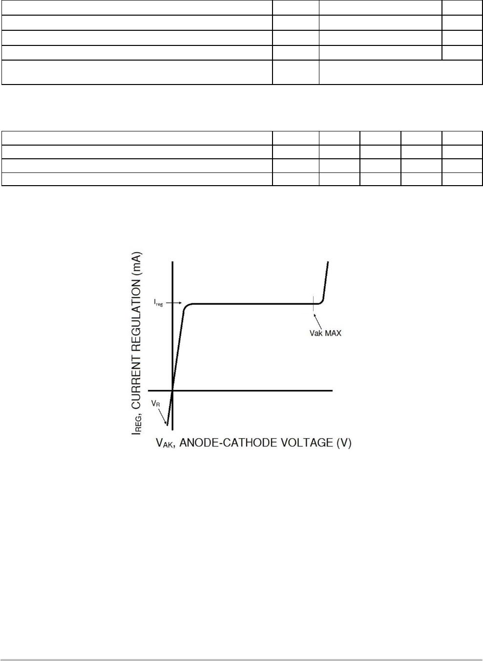
The linear constant current regulator (CCR) is a simple, economical
and robust device designed to provide a cost−effective solution for
regulating current in LEDs (similar to Constant Current Diode, CCD).
The CCR is based on Self−Biased Transistor (SBT) technology and
regulates current over a wide voltage range. It is designed with a
negative temperature coefficient to protect LEDs from thermal
runaway at extreme voltages and currents.
The CCR turns on immediately and is at 45% of regulation with
only 0.5 V Vak. It requires no external components allowing it to be
designed as a high or low−side regulator.
The 120 V anode−cathode voltage rating is designed to withstand
the high peak voltage incurred in A/C offline applications. The high
anode−cathode voltage rating withstands surges common in
Automotive, Industrial and Commercial Signage applications.
Features
• Robust Power Package: 3 W
• Wide Operating Voltage Range
• Immediate Turn-On
• Voltage Surge Suppressing − Protecting LEDs
• UL94−V0 Certified
• SBT (Self−Biased Transistor) Technology
• Negative Temperature Coefficient
• Also available in 50 mA (NSIC2050JBT3G) and 30 mA
(NSIC2030JBT3G)
• NSV Prefix for Automotive and Other Applications Requiring
Unique Site and Control Change Requirements; AEC−Q101
Qualified and PPAP Capable
• These Devices are Pb−Free, Halogen Free/BFR Free and are RoHS
Compliant
Typical Applications and Reference/Design Documents
• Automobile: Chevron Side Mirror Markers, Cluster, Displays &
Instruments Backlighting, CHMSL, Map Light
• AC Lighting Panels, Display Signage, Decorative Lighting, Channel
Lettering
• Application Note AND8349/D – Automotive CHMSL
• Application Notes AND8391/D, AND9008/D − Power Dissipation
Considerations
• Application Note AND8433/D – A/C Application
• Application Note AND8492/D – A/C Capacitive Drop Design
• Application Note AND9098/D − Protecting a CCR from ISO 7637−2
Pulse 2A and Reverse Pulses
• Design Note DN05013 – A/C Design
• Design Note DN06065 – A/C Design with PFC
http://onsemi.com
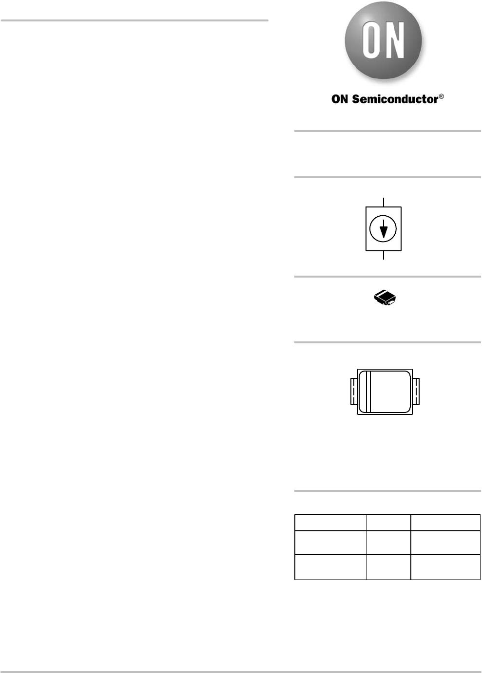
SMB
CASE 403A
MARKING DIAGRAM
Device Package Shipping
†
ORDERING INFORMATION
NSIC2020JBT3G SMB
(Pb−Free)
2500 / Tape &
Reel
†For information on tape and reel specifications,
including part orientation and tape sizes, please
refer to our Tape and Reel Packaging Specification
Brochure, BRD8011/D.
(Note: Microdot may be in either location)
I
reg(SS)
= 20 mA
@ Vak = 7.5 V
2020J = Specific Device Code
A = Assembly Location
Y = Year
WW = Work Week
G = Pb−Free Package
AYWW
2020JG
G
Anode 2
Cathode 1
1
2
12
NSVC2020JBT3G SMB
(Pb−Free)
2500 / Tape &
Reel