General Description
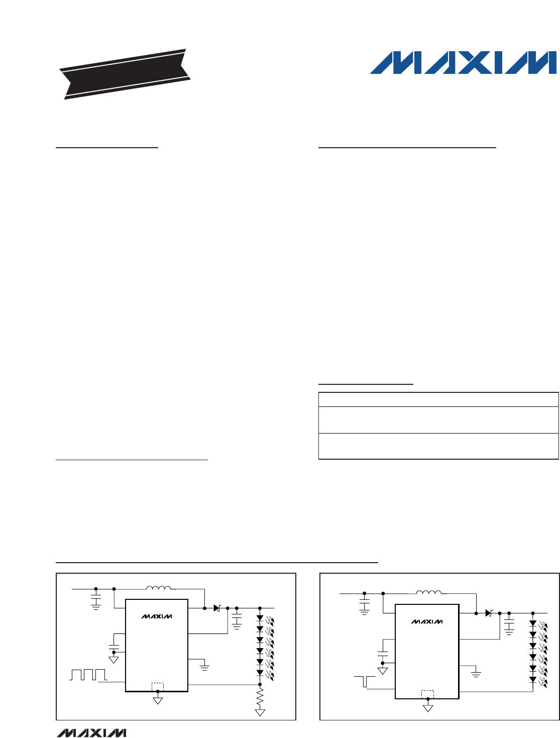
The MAX8901A/MAX8901B step-up converters drive from
two to six series-connected white LEDs (WLEDs) with
constant current to provide uniform WLED intensity for
LCD backlighting in cell phones, PDAs, and other hand-
held devices. The MAX8901_ operate at a fixed 750kHz
(typ) switching frequency, allowing for tiny external com-
ponents, and are optimized for the highest possible effi-
ciency over the full 1-cell Li+/Li-Poly battery range.
These converters use a single input (ON) to enable the
IC and to control WLED intensity. The MAX8901A
requires a direct PWM input to regulate WLED intensity
with the WLED current proportional to the PWM duty
cycle. The MAX8901B uses single-wire, serial-pulse
dimming that reduces the WLED intensity in 32 linear
steps. Full-scale WLED current for serial-pulse
dimming is 24.75mA (MAX8901B, 0.75mA/step).
The MAX8901_ feature an internal soft-start to eliminate
inrush currents during startup, input overvoltage
protection, WLED overvoltage protection, and a shut-
down mode with 0.01µA (typ) shutdown current. No
WLED current is present in shutdown provided the
WLED forward voltage is greater than the input supply
voltage. Additional features include undervoltage lock-
out (UVLO) and thermal shutdown.
The MAX8901_ are available in tiny 8-pin, 2mm x 2mm
TDFN-EP packages (0.8mm max height).
Applications
Display Backlight (from 2 to 6 WLEDs)
Cellular Phones
PDAs and Smartphones
MP3 and Portable Media Players
Portable Navigation Devices
Digital Cameras
Features
o High Efficiency, Up to 91%
o 2.6V to 5.5V Input Voltage Range
o Fixed-Frequency Operation
o Supplies from 2 to 6 WLEDs with 1.3% LED Current
Accuracy
o Flexible Dimming Control
Direct PWM Dimming (MAX8901A)
32-Step, Single-Wire Serial Dimming
(MAX8901B)
o Input Undervoltage Lockout
o Input Overvoltage Lockout
o WLED Overvoltage Protection (25V typ)
o 0.01µA (typ) Shutdown Current
o No WLED Current in Shutdown
o Internal Soft-Start and Thermal Shutdown
MAX8901A/MAX8901B
Highest Efficiency Supply for 2 to 6
Series WLEDs in a 2mm x 2mm TDFN Package
________________________________________________________________
Maxim Integrated Products
1
Ordering Information
MAX8901A
IN
COMP
GND
ON
LX
OVP
PGND
CS
OUTPUT
UP TO 25V
4
1
5
8
2
EP
3
7
6
INPUT
2.6V TO 5.5V
PWM DIMMING
CONTROL
Typical Operating Circuits
19-0865; Rev 3; 8/10
Note: All devices are specified over the -40°C to +85°C operating
temperature range.
+
Denotes a lead(Pb)-free/RoHS-compliant package.
*
EP = Exposed pad.
T = Tape and reel.
For pricing, delivery, and ordering information, please contact Maxim Direct at 1-888-629-4642,
or visit Maxim's website at www.maxim-ic.com.
EVALUATION KIT
AVAILABLE
PART PIN-PACKAGE TOP MARK
MAX8901AETA+T
8 TDFN-EP*
2mm x 2mm
+ABA
MAX8901BETA+T
8 TDFN-EP*
2mm x 2mm
+ABB
MAX8901B
IN
COMP
GND
ON
LX
OVP
PGND
CS
OUTPUT
UP TO 25V
4
1
5
8
2
EP
3
7
6
INPUT
2.6V TO 5.5V
SERIAL-PULSE
DIMMING
CONTROL
Pin Configuration appears at end of data sheet.
MAX8901A/MAX8901B
Highest Efficiency Supply for 2 to 6
Series WLEDs in a 2mm x 2mm TDFN Package
2 _______________________________________________________________________________________
ABSOLUTE MAXIMUM RATINGS
ELECTRICAL CHARACTERISTICS
(V
IN
= V
ON
= V
OVP
= 3.6V, V
PGND
= V
GND
= 0V, COMP, CS, and LX are unconnected, T
A
= -40°C to +85°C, unless otherwise noted.
Typical values are at T
A
= +25°C.) (Note 1)
Stresses beyond those listed under “Absolute Maximum Ratings” may cause permanent damage to the device. These are stress ratings only, and functional
operation of the device at these or any other conditions beyond those indicated in the operational sections of the specifications is not implied. Exposure to
absolute maximum rating conditions for extended periods may affect device reliability.
IN to GND .................................................................-0.3V to +7V
CS, COMP, ON to GND ...............................-0.3V to (V
IN
+ 0.3V)
OVP, LX to GND .....................................................-0.3V to +28V
PGND to GND .......................................................-0.3V to +0.3V
LX Current ..................................................................770mA
RMS
Continuous Power Dissipation (multilayer board at +70°C)
8-pin, 2mm x 2mm TDFN
(derate above +70°C by 11.9mW/°C)..........................953mW
Operating Temperature Range ...........................-40°C to +85°C
Junction Temperature......................................................+150°C
Storage Temperature Range .............................-65°C to +150°C
Lead Temperature (soldering, 10s) .................................+300°C
Soldering Temperature (reflow) .......................................+260°C
PARAMETER SYMBOL CONDITIONS MIN TYP MAX UNITS
Input Voltage V
IN
2.6 5.5 V
V
IN
rising 2.25 2.55
Input Undervoltage Lockout
Threshold
V
IN_UVLO
V
IN
falling 2.53
V
V
IN
rising 6.2 6.35
Input Overvoltage Lockout
Threshold
V
IN_OVLO
V
IN
falling 6.0 6.3
V
T
A
= +25°C 0.01 1
Shutdown Input Current I
SHDN
V
ON
= 0V
T
A
= +85°C 0.1
µA
MAX8901A 70 135
Quiescent Current I
Q
V
CS
= 0.55V, no load
(not switching)
MAX8901B 115 185
µA
Output Voltage Range V
OUT
V
DIODE
= external boost diode voltage drop
V
IN
-
V
DIODE
V
OV
V
OVP Overvoltage Protection
Threshold
V
OV
6 LEDs with 25V OVP option 24 25 26 V
OVP Input Current I
OV
V
OVP
= 20V 20 µA
CS Regulation Voltage V
CS
No dimming 0.475 0.50 0.525 V
ON Shutdown Delay t
SHDN
Time V
ON
is below low threshold until
shutdown (Figure 1)
1.18 1.33 1.50 ms
ON High Voltage V
ON_HI
2.6V < V
IN
< 5.5V 1.3 V
ON Low Voltage V
ON_LO
2.6V < V
IN
< 5.5V 0.4 V
T
A
= +25°C 0.01 1
ON Input Current I
ON
ON = IN
T
A
= +85°C 0.1
µA
Initial ON High Pulse Width t
HI_INIT
First ON high pulse to enable IC
(MAX8901B) (Figure 1)
40 µs
ON High Pulse Width t
HI
MAX8901B (Figure 1) 0.5 µs
ON Low Pulse Width t
LO
MAX8901B (Figure 1) 0.5 500.0 µs
MAX8901A/MAX8901B
Highest Efficiency Supply for 2 to 6
Series WLEDs in a 2mm x 2mm TDFN Package
_______________________________________________________________________________________ 3
Note 1: Specifications to -40°C are guaranteed by design and characterization and are not production tested.
PARAMETER SYMBOL CONDITIONS MIN TYP MAX UNITS
T
A
= +25°C -1.3 +1.3 %
Serial Dimming
Full-Scale LED Current Accuracy
I
LED
= 24.75mA
(MAX8901B)
T
A
= -40°C to +85°C-3 +3 %
PWM Frequency for PWM
Dimming Control
f
PWM
MAX8901A 100 kHz
CS to COMP Transconductance 40 60 80 µS
Soft-Start Interval
t
SOFT-
START
C
COMP
= 0.022µF (Figure 1) 10 ms
Thermal Shutdown 160 °C
OSCILLATOR
Operating Frequency f
SW
700 750 800 kHz
Maximum Duty Cycle D
MAX
V
CS
= 0.4V 90 92 %
n-CHANNEL SWITCH
T
A
= +25°C 0.1 5
LX Leakage Current I
LXLKG
V
LX
= 27V
T
A
= +85°C 0.1
µA
n-Channel Switch On-Resistance R
LX
0.7 1.4 Ω
n-Channel Current Limit I
LIM
0.63 0.70 0.77 A
ELECTRICAL CHARACTERISTICS (continued)
(V
IN
= V
ON
= V
OVP
= 3.6V, V
PGND
= V
GND
= 0V, COMP, CS, and LX are unconnected, T
A
= -40°C to +85°C, unless otherwise noted.
Typical values are at T
A
= +25°C.) (Note 1)
1
0
2 3 4 5 28 29 30 31 32
SHUTDOWN
t
SHDN
1.33ms (typ)
2/33
1/33
3/33
4/33
5/33
6/33
28/33
29/33
30/33
31/33
32/33
32/33
SHUTDOWN
FULL
FULL
I
LED_
t
SOFT-START
t
HI_INIT
t
LO
t
HI
> 40μs
> 500ns
500ns TO 500μs
STEP
33
ON
Figure 1. MAX8901B Timing Diagram

MAX8901BETA+TCH8

Mfr. #:
Manufacturer:
Maxim Integrated
Description:
LED Lighting Drivers Supply for 2 to 6 Series WLEDs
Lifecycle:
New from this manufacturer.
Delivery:
DHL FedEx Ups TNT EMS
Payment:
T/T Paypal Visa MoneyGram Western Union

Products related to this Datasheet