TCET1107

www.vishay.com For technical questions, contact: optocoupleranswers@vishay.com
Document Number: 83503
810 Rev. 2.3, 14-Oct-09
TCET1100, TCET1100G
Vishay Semiconductors
Optocoupler, Phototransistor Output, High Temperature
DESCRIPTION
The TCET110. consists of a phototransistor optically coupled
to a gallium arsenide infrared-emitting diode in a 4-lead
plastic dual inline package.
AGENCY APPROVALS
UL1577, file no. E52744, double protection
cUL tested, file A52744
BSI: EN 60065:2002, EN 60950:2000
DIN EN 60747-5-5 (VDE 0884)
•FIMKO
FEATURES
High common mode rejection
Low temperature coefficient of CTR
CTR offered in 9 groups
Reinforced isolation provides circuit protection
against electrical shock (safety class II)
Isolation materials according to UL 94 V-O
Pollution degree 2 (DIN/VDE 0110/resp. IEC 60664)
Climatic classification 55/100/21 (IEC 60068 part 1)
Rated impulse voltage (transient overvoltage)
V
IOTM
= 6 kV
peak
Isolation test voltage (partial discharge test voltage)
V
pd
= 1.6 kV
Rated isolation voltage (RMS includes DC)
V
IOWM
= 600 V
RMS
Rated recurring peak voltage (repetitive)
V
IORM
= 848 V
peak
Creepage current resistance according to VDE 0303/
IEC 60112 comparative tracking index: CTI 175
Compliant to RoHS directive 2002/95/EC and in
accordance to WEEE 2002/96/EC
APPLICATIONS
Circuits for safe protective separation against electrical
shock according to safety class II (reinforced isolation):
for appl. class I - IV at mains voltage 300 V
for appl. class I - III at mains voltage 600 V according to
DIN EN 60747-5-5 (VDE 0884), suitable for:
- Switch-mode power supplies
- Line receiver
- Computer peripheral interface
- Microprocessor system interface
17197_5
C
E
AC
12
3
4
V
DE
C
17197_4
Document Number: 83503 For technical questions, contact: optocoupleranswers@vishay.com
www.vishay.com
Rev. 2.3, 14-Oct-09 811
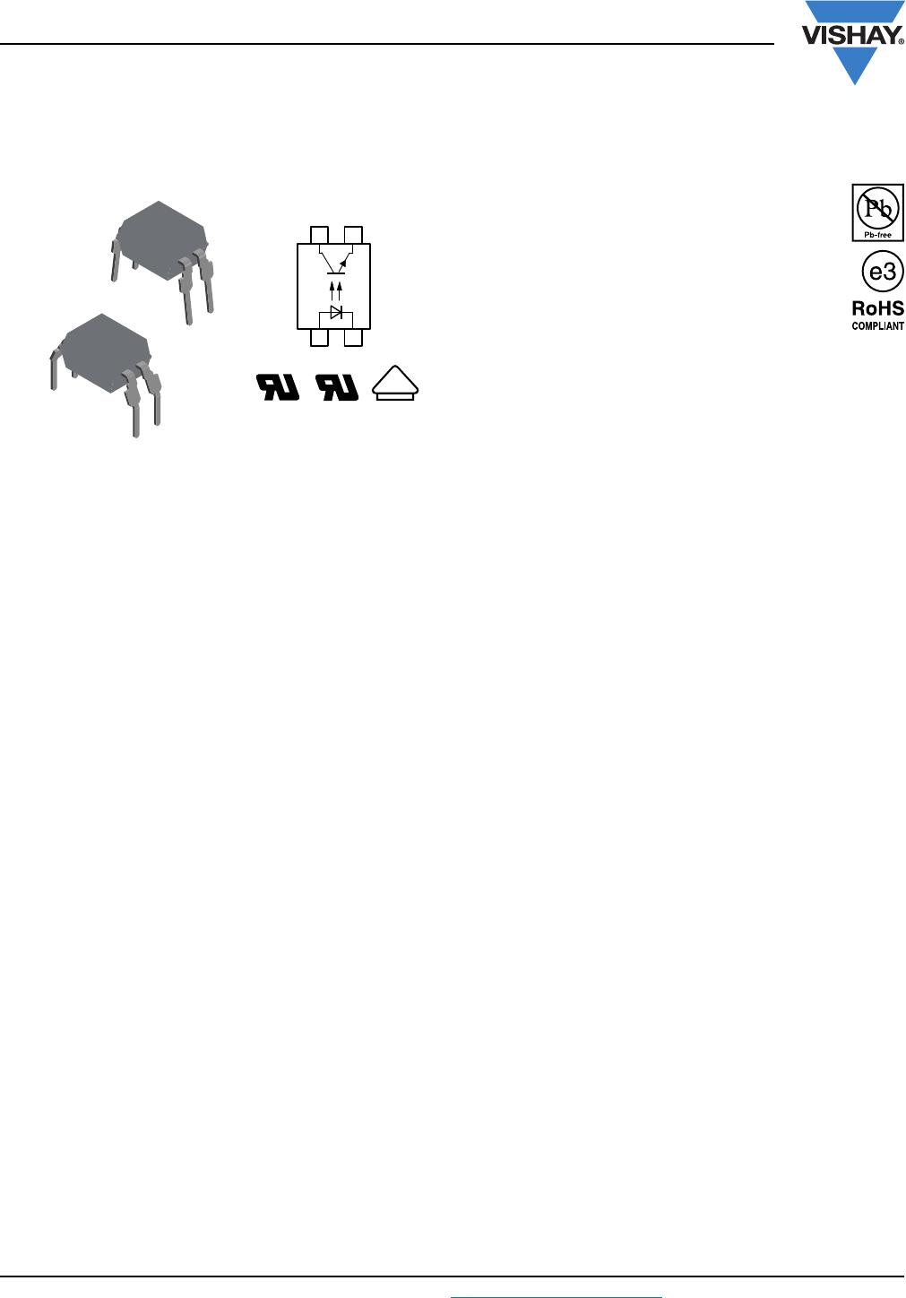
TCET1100, TCET1100G
Optocoupler, Phototransistor Output,
High Temperature
Vishay Semiconductors
Note
G = lead form 10.16 mm; G is not marked on the body
Notes
(1)
T
amb
= 25 °C, unless otherwise specified.
Stresses in excess of the absolute maximum ratings can cause permanent damage to the device. Functional operation of the device is not
implied at these or any other conditions in excess of those given in the operational sections of this document. Exposure to absolute maximum
ratings for extended periods of the time can adversely affect reliability.
(2)
Refer to wave profile for soldering conditions for through hole devices (DIP).
ORDER INFORMATION
PART REMARKS
TCET1100 CTR 50 % to 600 %, DIP-4
TCET1101 CTR 40 % to 80 %, DIP-4
TCET1102 CTR 63 % to 125 %, DIP-4
TCET1103 CTR 100 % to 200 %, DIP-4
TCET1104 CTR 160 % to 320 %, DIP-4
TCET1105 CTR 50 % to 150 %, DIP-4
TCET1106 CTR 100 % to 300 %, DIP-4
TCET1107 CTR 80 % to 160 %, DIP-4
TCET1108 CTR 130 % to 260 %, DIP-4
TCET1109 CTR 200 % to 400 %, DIP-4
TCET1100G CTR 50 % to 600 %, DIP-4, 400 mil
TCET1101G CTR 40 % to 80 %, DIP-4, 400 mil
TCET1102G CTR 63 % to 125 %, DIP-4, 400 mil
TCET1103G CTR 100 % to 200 %, DIP-4, 400 mil
TCET1104G CTR 160 % to 320 %, DIP-4, 400 mil
TCET1105G CTR 50 % to 150 %, DIP-4, 400 mil
TCET1106G CTR 100 % to 300 %, DIP-4, 400 mil
TCET1107G CTR 80 % to 160 %, DIP-4, 400 mil
TCET1108G CTR 130 % to 260 %, DIP-4, 400 mil
TCET1109G CTR 200 % to 400 %, DIP-4, 400 mil
ABSOLUTE MAXIMUM RATINGS
(1)
PARAMETER TEST CONDITION SYMBOL VALUE UNIT
INPUT
Reverse voltage V
R
6V
Forward current I
F
60 mA
Forward surge current t
p
10 µs I
FSM
1.5 A
OUTPUT
Collector emitter voltage V
CEO
70 V
Emitter collector voltage V
ECO
7V
Collector current I
C
50 mA
Collector peak current t
p
/T = 0.5, t
p
10 ms I
CM
100 mA
COUPLER
Isolation test voltage (RMS) t = 1 min V
ISO
5000 V
RMS
Operating ambient temperature range T
amb
- 40 to + 100 °C
Storage temperature range T
stg
- 55 to + 125 °C
Soldering temperature
(2)
2 mm from case, 10 s T
sld
260 °C
www.vishay.com For technical questions, contact: optocoupleranswers@vishay.com
Document Number: 83503
812 Rev. 2.3, 14-Oct-09
TCET1100, TCET1100G
Vishay Semiconductors
Optocoupler, Phototransistor Output,
High Temperature
Note
(1)
The thermal model is represented in the thermal network below. Each resistance value given in this model can be used to calculate the
temperatures at each node for a given operating condition. The thermal resistance from board to ambient will be dependent on the type of
PCB, layout and thickness of copper traces. For a detailed explanation of the thermal model, please reference Vishay’s “Thermal
Characteristics of Optocouplers” application note.
(2)
For 2 layer FR4 board (4" x 3" x 0.062").
Note
T
amb
= 25 °C, unless otherwise specified.
Minimum and maximum values are testing requirements. Typical values are characteristics of the device and are the result of engineering
evaluation. Typical values are for information only and are not part of the testing requirements.
THERMAL CHARACTERISTICS
(1)
PARAMETER SYMBOL VALUE UNIT
LED power dissipation P
diss
100 mW
Output power dissipation P
diss
150 mW
Maximum LED junction temperature T
jmax.
125 °C
Maximum output die junction temperature T
jmax.
125 °C
Thermal resistance, junction emitter to board θ
EB
173 °C/W
Thermal resistance, junction emitter to case θ
EC
149 °C/W
Thermal resistance, junction detector to board θ
DB
111 °C/W
Thermal resistance, junction detector to case θ
DC
127 °C/W
Thermal resistance, junction emitter to
junction detector
θ
ED
173 °C/W
Thermal resistance, board to ambient
(2)
θ
BA
197 °C/W
Thermal resistance, case to ambient
(2)
θ
CA
4041 °C/W
ELECTRICAL CHARACTERISTICS
PARAMETER TEST CONDITION SYMBOL MIN. TYP. MAX. UNIT
INPUT
Forward voltage I
F
= 50 mA V
F
1.25 1.6 V
Junction capacitance V
R
= 0, f = 1 MHz C
j
50 pF
OUTPUT
Collector emitter voltage I
C
= 1 mA V
CEO
70 V
Emitter collector voltage I
E
= 100 µA V
ECO
7V
Collector emitter cut-off current V
CE
= 20 V, I
F
= 0 A, E = 0 I
CEO
10 100 nA
COUPLER
Collector emitter saturation voltage I
F
= 10 mA, I
C
= 1 mA V
CEsat
0.3 V
Cut-off frequency V
CE
= 5 V, I
F
= 10 mA, R
L
= 100 Ω f
c
110 kHz
Coupling capacitance f = 1 MHz C
k
0.3 pF
T
A
θ
CA
T
C
T
JD
T
JE
T
B
θ
EC
θ
EB
θ
DC
θ
DB
θ
BA
θ
DE
T
A
19996
Package

TCET1107

Mfr. #:
Manufacturer:
Vishay Semiconductors
Description:
Transistor Output Optocouplers Phototransistor Out
Lifecycle:
New from this manufacturer.
Delivery:
DHL FedEx Ups TNT EMS
Payment:
T/T Paypal Visa MoneyGram Western Union