TCET1107

Document Number: 83503 For technical questions, contact: optocoupleranswers@vishay.com
www.vishay.com
Rev. 2.3, 14-Oct-09 813
TCET1100, TCET1100G
Optocoupler, Phototransistor Output,
High Temperature
Vishay Semiconductors
Note
According to DIN EN 60747-5-5 (see figure 2). This optocoupler is suitable for safe electrical isolation only within the safety ratings. Compliance
with the safety ratings shall be ensured by means of suitable protective circuits.
CURRENT TRANSFER RATIO
PARAMETER TEST CONDITION PART SYMBOL MIN. TYP. MAX. UNIT
I
C
/I
F
V
CE
= 5 V, I
F
= 1 mA
TCET1101
TCET1101G
CTR 13 30 %
TCET1102
TCET1102G
CTR 22 45 %
TCET1103
TCET1103G
CTR 34 70 %
TCET1104
TCET1104G
CTR 56 90 %
V
CE
= 5 V, I
F
= 5 mA
TCET1100
TCET1100G
CTR 50 600 %
TCET1105
TCET1105G
CTR 50 150 %
TCET1106
TCET1106G
CTR 100 300 %
TCET1107
TCET1107G
CTR 80 160 %
TCET1108
TCET1108G
CTR 130 260 %
TCET1109
TCET1109G
CTR 200 400 %
V
CE
= 5 V, I
F
= 10 mA
TCET1101
TCET1101G
CTR 40 80 %
TCET1102
TCET1102G
CTR 63 125 %
TCET1103
TCET1103G
CTR 100 200 %
TCET1104
TCET1104G
CTR 160 320 %
MAXIMUM SAFETY RATINGS
PARAMETER TEST CONDITION SYMBOL MIN. TYP. MAX. UNIT
INPUT
Forward current I
F
130 mA
OUTPUT
Power dissipation P
diss
265 mW
COUPLER
Rated impulse voltage V
IOTM
6kV
Safety temperature T
si
150 °C
INSULATION RATED PARAMETERS
PARAMETER TEST CONDITION SYMBOL MIN. TYP. MAX. UNIT
Partial discharge test voltage -
routine test
100 %, t
test
= 1 s V
pd
1.6 kV
Partial discharge test voltage -
lot test (sample test)
t
Tr
= 60 s, t
test
= 10 s,
(see figure 2)
V
IOTM
6kV
V
pd
1.3 kV
Insulation resistance
V
IO
= 500 V R
IO
10
12
Ω
V
IO
= 500 V, T
amb
= 100 °C R
IO
10
11
Ω
V
IO
= 500 V, T
amb
= 150 °C
(construction test only)
R
IO
10
9
Ω
www.vishay.com For technical questions, contact: optocoupleranswers@vishay.com
Document Number: 83503
814 Rev. 2.3, 14-Oct-09
TCET1100, TCET1100G
Vishay Semiconductors
Optocoupler, Phototransistor Output,
High Temperature
Fig. 1 - Derating Diagram Fig. 2 - Test Pulse Diagram for Sample Test According to
DIN EN 60747-5-5/DIN EN 60747-; IEC 60747
Fig. 3 - Test Circuit, Non-Saturated Operation Fig. 4 - Test Circuit, Saturated Operation
0 25 50 75 125
0
50
100
150
200
300
P
tot
- Total Power Dissipation (mW)
T
si
- Safety Temperature (°C)
150
94 9182
100
250
Phototransistor
P
si
(mW)
IR-diode
I
si
(mA)
t
13930
t
1
, t
2
= 1 to 10 s
t
3
, t
4
= 1 s
t
test
= 10 s
t
stres
= 12 s
V
IOTM
V
Pd
V
IOWM
V
IORM
0
t
1
t
test
t
Tr
= 60 s
t
stres
t
3
t
4
t
2
SWITCHING CHARACTERISTICS
PARAMETER TEST CONDITION SYMBOL MIN. TYP. MAX. UNIT
Delay time
V
S
= 5 V, I
C
= 2 mA, R
L
= 100 Ω,
(see figure 3)
t
d
s
Rise time
V
S
= 5 V, I
C
= 2 mA, R
L
= 100 Ω,
(see figure 3)
t
r
s
Turn-on time
V
S
= 5 V, I
C
= 2 mA, R
L
= 100 Ω,
(see figure 3)
t
on
s
Storage time
V
S
= 5 V, I
C
= 2 mA, R
L
= 100 Ω,
(see figure 3)
t
s
0.3 µs
Fall time
V
S
= 5 V, I
C
= 2 mA, R
L
= 100 Ω,
(see figure 3)
t
f
4.7 µs
Turn-off time
V
S
= 5 V, I
C
= 2 mA, R
L
= 100 Ω,
(see figure 3)
t
off
s
Turn-on time
V
S
= 5 V, I
F
= 10 mA, R
L
= 1 kΩ,
(see figure 4)
t
on
s
Turn-off time
V
S
= 5 V, I
F
= 10 mA, R
L
= 1 kΩ,
(see figure 4)
t
off
10 µs
Channel I
Channel II
95 10804
R
G
= 50 Ω
t
p
t
p
= 50 µs
T
= 0.01
+ 5 V
I
F
0
50 Ω 100 Ω
I
F
I
C
= 2 mA; adjusted through
input amplitude
Oscilloscope
R
L
= 1 MΩ
C
L
= 20 pF
Channel I
Channel II
95 10843
R
G
= 50 Ω
t
p
t
p
= 50 µs
T
= 0.01
+ 5 V
I
C
I
F
0
50 Ω
1 kΩ
I
F
= 10 mA
Oscilloscope
R
L
C
L
20 pF
1 MΩ
Document Number: 83503 For technical questions, contact: optocoupleranswers@vishay.com
www.vishay.com
Rev. 2.3, 14-Oct-09 815
TCET1100, TCET1100G
Optocoupler, Phototransistor Output,
High Temperature
Vishay Semiconductors
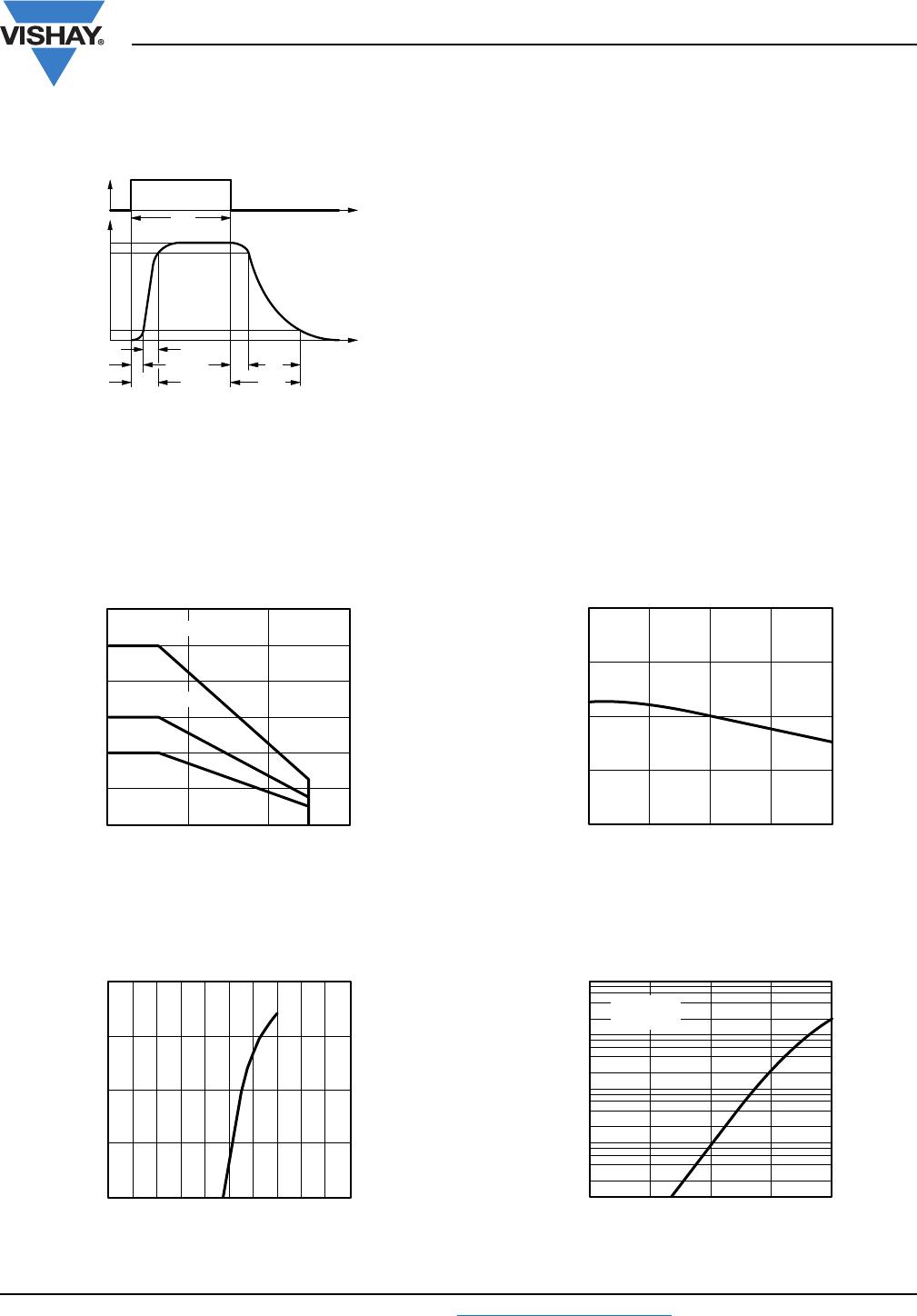
Fig. 5 - Switching Times
TYPICAL CHARACTERISTICS
T
amb
= 25 °C, unless otherwise specified
Fig. 6 - Total Power Dissipation vs. Ambient Temperature
Fig. 7 - Forward Current vs. Forward Voltage
Fig. 8 - Relative Current Transfer Ratio vs.
Ambient Temperature
Fig. 9 - Collector Dark Current vs. Ambient Temperature
t
p
t
t
0
0
10 %
90 %
100 %
t
r
t
d
t
on
t
s
t
f
t
off
I
F
I
C
t
p
Pulse duration
t
d
Delay time
t
r
Rise time
t
on
(= t
d
+ t
r
) Turn-on time
t
s
Storage time
t
f
Fall time
t
off
(= t
s
+ t
f
)Turn-off time
96 11698
0
50
100
150
200
250
300
04080 120
P
tot
- Total Power Dissipation (mW)
T
amb
- Ambient Temperature (°C)
96 11700
Coupled device
Phototransistor
IR-diode
0.1
1
10
100
1000
0
V
F
- Forward Voltage (V)
96 11862
I
F
- Forward Current (mA)
1.6
1.2
0.8
0.4
2.0
- 25 0 25 50
0
0.5
1.0
1.5
2.0
CTR
rel
- Relative Current Transfer Ratio
95 11025
75
T
amb
- Ambient Temperature (°C)
V
CE
= 5 V
I
F
= 5 mA
0255075
1
10
100
1000
10 000
I
CEO
- Collector Dark Current,
100
95 11026
with Open Base (nA)
V
CE
= 20 V
I
F
= 0
T
amb
- Ambient Temperature (°C)

TCET1107

Mfr. #:
Manufacturer:
Vishay Semiconductors
Description:
Transistor Output Optocouplers Phototransistor Out
Lifecycle:
New from this manufacturer.
Delivery:
DHL FedEx Ups TNT EMS
Payment:
T/T Paypal Visa MoneyGram Western Union