LTC3559/LTC3559-1
16
3559fb
APPLICATIONS INFORMATION
Solving these equations for R
NTC|COLD
and R
NTC|HOT
results in the following:
R
NTC|HOT
= 0.536 • R
NOM
and
R
NTC|COLD
= 3.25 • R
NOM
By setting R
NOM
equal to R25, the above equations result
in r
HOT
= 0.536 and r
COLD
= 3.25. Referencing these ratios
to the Vishay Resistance-Temperature Curve 1 chart gives
a hot trip point of about 40°C and a cold trip point of about
0°C. The difference between the hot and cold trip points
is approximately 40°C.
By using a bias resistor, R
NOM
, different in value from
R25, the hot and cold trip points can be moved in either
direction. The temperature span will change somewhat due
to the nonlinear behavior of the thermistor. The following
equations can be used to easily calculate a new value for
the bias resistor:
R
r
R
R
r
R
NOM
HOT
NOM
COLD
=
=
0 536
25
325
25
.
.
where r
HOT
and r
COLD
are the resistance ratios at the
de-
sired
hot and cold trip points. Note that these equations
are linked. Therefore, only one of the two trip points can
be chosen, the other is determined by the default ratios
designed in the IC. Consider an example where a 60°C
hot trip point is desired.
From the Vishay Curve 1 R-T characteristics, r
HOT
is 0.2488
at 60°C. Using the above equation, R
NOM
should be set
to 46.4k. With this value of R
NOM
, the cold trip point is
about 16°C. Notice that the span is now 44°C rather than
the previous 40°C.
The upper and lower temperature trip points can be inde-
pendently programmed by using an additional bias resistor
as shown in Figure 4. The following formulas can be used
to compute the values of R
NOM
and R
1
:
R
rr
R
RRr
NOM
COLD HOT
NOM HOT
=
=
.
.•
2 714
25
1 0 536 RR25
For example, to set the trip points to 0°C and 45°C with
a Vishay Curve 1 thermistor choose:
Rkk
NOM
==
3 266 0 4368
2 714
100 104 2
.–.
.
•.
the nearest 1% value is 105k.
R1 = 0.536 • 105k – 0.4368 • 100k = 12.6k
the nearest 1% value is 12.7k. The fi nal solution is shown
in Figure 4 and results in an upper trip point of 45°C and
a lower trip point of 0°C.
USB and Wall Adapter Power
Although the battery charger is designed to draw power
from a USB port to charge Li-Ion batteries, a wall adapter
can also be used. Figure 5 shows an example of how to
combine wall adapter and USB power inputs. A P-channel
MOSFET, MP1, is used to prevent back conduction into
the USB port when a wall adapter is present and Schottky
diode, D1, is used to prevent USB power loss through the
1k pull-down resistor.
Typically, a wall adapter can supply signifi cantly more
current than the 500mA-limited USB port. Therefore, an
N-channel MOSFET, MN1, and an extra program resistor are
used to increase the maximum charge current to 950mA
when the wall adapter is present.
V
CC
MP1
MN1
1k
1.74k
1.65k
I
BAT
Li-Ion
BATTER
Y
3559 F05
BATTERY
CHARGER
BAT
USB
POWER
500mA I
CHG
5V WALL
ADAPTER
950mA I
CHG
PROG
+
D1
Figure 5. Combining Wall Adapter and USB Power
LTC3559/LTC3559-1
17
3559fb
Power Dissipation
The conditions that cause the LTC3559/LTC3559-1 to
reduce charge current through thermal feedback can be
approximated by considering the power dissipated in the
IC. For high charge currents, the LTC3559/LTC3559-1
power dissipation is approximately:
PVV I
D CC BAT BAT
=
()
–•
where P
D
is the power dissipated, V
CC
is the input supply
voltage, V
BAT
is the battery voltage, and I
BAT
is the charge
current. It is not necessary to perform any worst-case power
dissipation scenarios because the LTC3559/LTC3559-1
will automatically reduce the charge current to maintain
the die temperature at approximately 105°C. However, the
approximate ambient temperature at which the thermal
feedback begins to protect the IC is:
TCP
TCVVI
ADJA
A CC BAT BAT J A
()
105
105
––
θ
θ
Example: Consider an LTC3559/LTC3559-1 operating from
a USB port providing 500mA to a 3.5V Li-Ion battery.
The ambient temperature above which the LTC3559/
LTC3559-1 will begin to reduce the 500mA charge cur-
rent is approximately:
TCVVmACW
TC
A
A
()()
°
105 5 3 5 500 68
105 0
––. /
–.. / 75 68 105 51
54
WCW C
TC
A
°=° °
The LTC3559/LTC3559-1 can be used above 70°C, but
the charge current will be reduced from 500mA. The
approximate current at a given ambient temperature can
be calculated:
I
CT
VV
BAT
A
CC BAT JA
=
°
()
105
–•θ
Using the previous example with an ambient tem-
perature of 88°C, the charge current will be reduced to
approximately:
I
CC
VV CW
C
CA
BAT
=
°°
()
°
=
°
°
105 88
535 68
17
102
–. / /
IImA
BAT
= 167
APPLICATIONS INFORMATION
Furthermore, the voltage at the PROG pin will change
proportionally with the charge current as discussed in
the Programming Charge Current section.
It is important to remember that LTC3559/LTC3559-1
applications do not need to be designed for worst-case
thermal conditions since the IC will automatically reduce
power dissipation when the junction temperature reaches
approximately 105°C.
Battery Charger Stability Considerations
The LTC3559/LTC3559-1 battery charger contains two
control loops: the constant-voltage and constant-cur-
rent loops. The constant-voltage loop is stable without
any compensation when a battery is connected with low
impedance leads. Excessive lead length, however, may add
enough series inductance to require a bypass capacitor
of at least 1.5μF from BAT to GND. Furthermore, a 4.7μF
capacitor with a 0.2Ω to 1Ω series resistor from BAT to
GND is required to keep ripple voltage low when the bat-
tery is disconnected.
High value capacitors with very low ESR (especially
ceramic) reduce the constant-voltage loop phase margin,
possibly resulting in instability. Ceramic capacitors up to
22μF may be used in parallel with a battery, but larger
ceramics should be decoupled with 0.2Ω to 1Ω of series
resistance.
In constant-current mode, the PROG pin is in the feedback
loop, not the battery. Because of the additional pole created
by the PROG pin capacitance, capacitance on this pin must
be kept to a minimum. With no additional capacitance on
the PROG pin, the charger is stable with program resistor
values as high as 25K. However, additional capacitance
on this node reduces the maximum allowed program
resistor. The pole frequency at the PROG pin should be
kept above 100kHz. Therefore, if the PROG pin is loaded
with a capacitance, C
PROG
, the following equation should
be used to calculate the maximum resistance value for
R
PROG
:
R
C
PROG
PROG
1
210
5
π ••
LTC3559/LTC3559-1
18
3559fb
APPLICATIONS INFORMATION
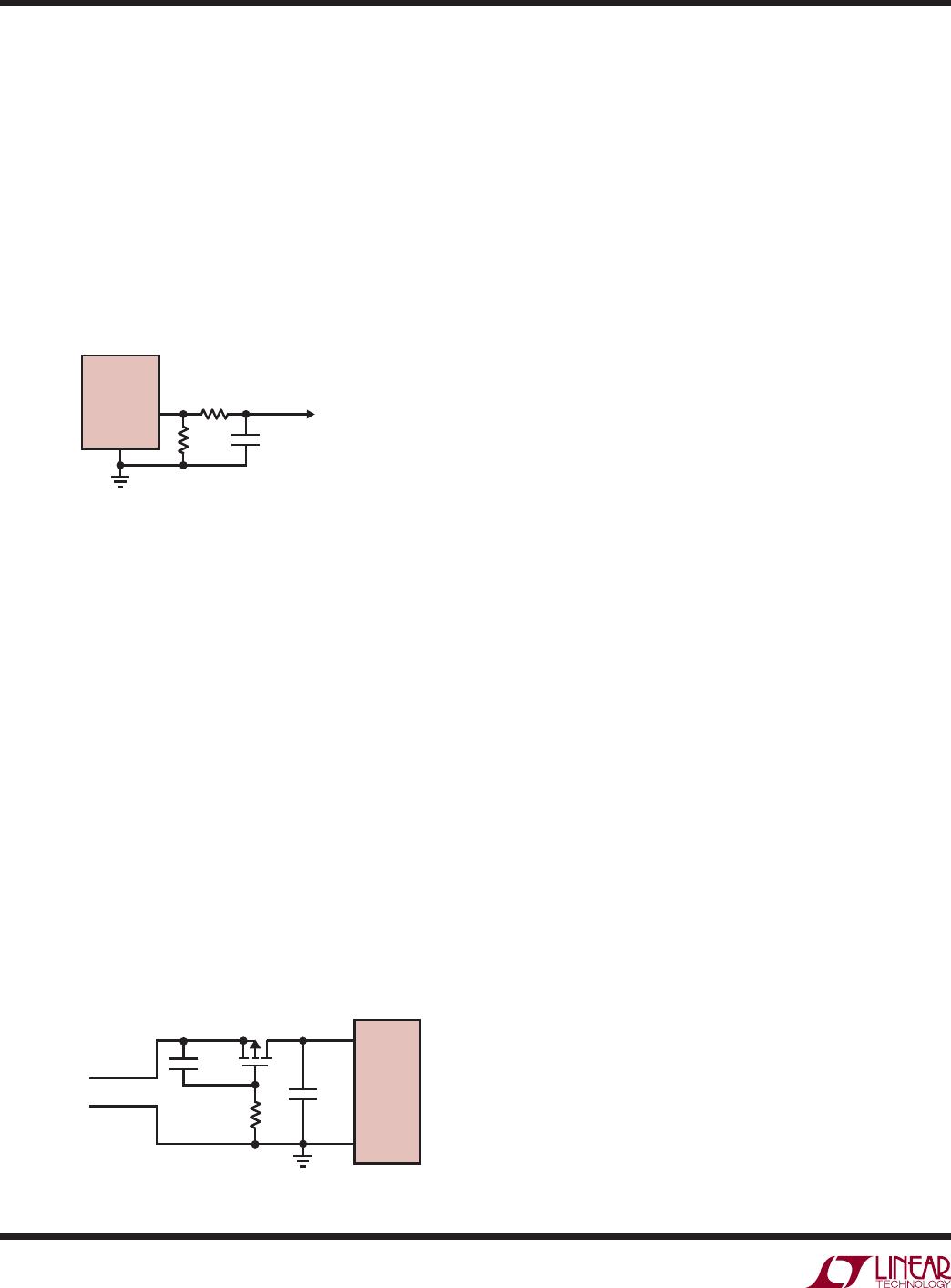
Average, rather than instantaneous, battery current may be
of interest to the user. For example, if a switching power
supply operating in low-current mode is connected in
parallel with the battery, the average current being pulled
out of the BAT pin is typically of more interest than the
instantaneous current pulses. In such a case, a simple RC
lter can be used on the PROG pin to measure the average
battery current as shown in Figure 6. A 10k resistor has
been added between the PROG pin and the fi lter capacitor
to ensure stability.
the current from building up in the cable too fast thus
dampening out any resonant overshoot.
Buck Switching Regulator General Information
The LTC3559/LTC3559-1 contain two 2.25MHz constant-
frequency current mode switching regulators that provide
up to 400mA each. Both switchers can be programmed
for a minimum output voltage of 0.8V and can be used
to power a microcontroller core, microcontroller I/O,
memory or other logic circuitry. Both regulators support
100% duty cycle operation (dropout mode) when the
input voltage drops very close to the output voltage and
are also capable of operating in Burst Mode operation for
highest effi ciencies at light loads (Burst Mode operation
is pin selectable). The switching regulators also include
soft-start to limit inrush current when powering on, short
circuit current protection, and switch node slew limiting
circuitry to reduce radiated EMI.
A single MODE pin sets both regulators in Burst Mode
operation or pulse skip operating mode while each regula-
tor is enabled individually through their respective enable
pins EN1 and EN2. The buck regulators input supply (PV
IN
)
should be connected to the battery pin (BAT). This allows
the undervoltage lockout circuit on the BAT pin to disable
the buck regulators when the BAT voltage drops below
2.45V. Do not drive the buck switching regulators from
a voltage other than BAT. A 2.2μF decoupling capacitor
from the PV
IN
pin to GND is recommended.
Buck Switching Regulator
Output Voltage Programming
Both switching regulators can be programmed for output
voltages greater than 0.8V. The output voltage for each
buck switching regulator is programmed using a resistor
divider from the switching regulator output connected to
the feedback pins (FB1 and FB2) such that:
V
OUT
= 0.8(1 + R1/R2)
Typical values for R1 are in the range of 40k to 1M. The
capacitor C
FB
cancels the pole created by feedback re-
sistors and the input capacitance of the FB pin and also
helps to improve transient response for output voltages
much greater than 0.8V. A variety of capacitor sizes can
be used for C
FB
but a value of 10pF is recommended for
3559 F06
C
FILTER
CHARGE
CURRENT
MONITOR
CIRCUITRY
R
PROG
LTC3559/
LTC3559-1
PROG
GND
10k
Figure 6. Isolated Capacitive Load on PROG Pin and Filtering
USB Inrush Limiting
When a USB cable is plugged into a portable product,
the inductance of the cable and the high-Q ceramic input
capacitor form an L-C resonant circuit. If there is not
much impedance in the cable, it is possible for the voltage
at the input of the product to reach as high as twice the
USB voltage (~10V) before it settles out. In fact, due to
the high voltage coeffi cient of many ceramic capacitors
(a nonlinearity), the voltage may even exceed twice the
USB voltage. To prevent excessive voltage from damaging
the LTC3559/LTC3559-1 during a hot insertion, the soft
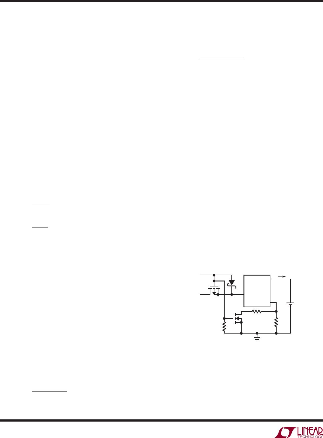
connect circuit in Figure 7 can be employed.
In the circuit of Figure 7, capacitor C1 holds MP1 off when
the cable is fi rst connected. Eventually C1 begins to charge
up to the USB voltage applying increasing gate support
to MP1. The long time constant of R1 and C1 prevents
Figure 7. USB Soft Connect Circuit
R1
40k
5V USB
INPUT
3559 F07
C1
100nF
C2
10μF
MP1
Si2333
USB CABLE
V
CC
GND
LTC3559/
LTC3559-1

LTC3559EUD-1#PBF

Mfr. #:
Manufacturer:
Analog Devices / Linear Technology
Description:
Battery Management Low Power USB Charger, Dual Buck Regulator in 3x3 DFN
Lifecycle:
New from this manufacturer.
Delivery:
DHL FedEx Ups TNT EMS
Payment:
T/T Paypal Visa MoneyGram Western Union