LTC3559/LTC3559-1
19
3559fb
APPLICATIONS INFORMATION
most applications. Experimentation with capacitor sizes
between 2pF and 22pF may yield improved transient
response if so desired by the user.
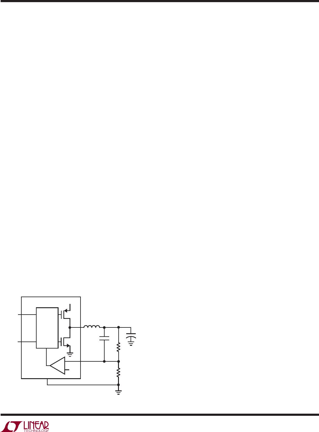
Buck Switching Regulator Operating Modes
The step-down switching regulators include two possible
operating modes to meet the noise/power needs of a
variety of applications.
In pulse skip mode, an internal latch is set at the start of
every cycle, which turns on the main P-channel MOSFET
switch. During each cycle, a current comparator compares
the peak inductor current to the output of an error amplifi er.
The output of the current comparator resets the internal
latch, which causes the main P-channel MOSFET switch to
turn off and the N-channel MOSFET synchronous rectifi er
to turn on. The N-channel MOSFET synchronous rectifi er
turns off at the end of the 2.25MHz cycle or if the current
through the N-channel MOSFET synchronous rectifi er
drops to zero. Using this method of operation, the error
amplifi er adjusts the peak inductor current to deliver the
required output power. All necessary compensation is
internal to the step-down switching regulator requiring
only a single ceramic output capacitor for stability. At
light loads in pulse skip mode, the inductor current may
reach zero on each pulse which will turn off the N-channel
MOSFET synchronous rectifi er. In this case, the switch
node (SW1 or SW2) goes high impedance and the switch
node voltage will “ring”. This is discontinuous operation,
and is normal behavior for a switching regulator. At very
light loads in pulse skip mode, the step-down switching
regulators will automatically skip pulses as needed to
maintain output regulation. At high duty cycle (V
OUT
>
PV
IN
/2) in pulse skip mode, it is possible for the inductor
current to reverse causing the buck converter to switch
continuously. Regulation and low noise operation are
maintained but the input supply current will increase to a
couple mA due to the continuous gate switching.
During Burst Mode operation, the step-down switching
regulators automatically switch between fi xed frequency
PWM operation and hysteretic control as a function of
the load current. At light loads the step-down switching
regulators control the inductor current directly and use a
hysteretic control loop to minimize both noise and switching
losses. During Burst Mode operation, the output capacitor
is charged to a voltage slightly higher than the regulation
point. The step-down switching regulator then goes into
sleep mode, during which the output capacitor provides
the load current. In sleep mode, most of the switching
regulators circuitry is powered down, helping conserve
battery power. When the output voltage drops below a
pre-determined value, the step-down switching regulator
circuitry is powered on and another burst cycle begins. The
sleep time decreases as the load current increases. Beyond
a certain load current point (about 1/4 rated output load
current) the step-down switching regulators will switch to
a low noise constant frequency PWM mode of operation,
much the same as pulse skip operation at high loads. For
applications that can tolerate some output ripple at low
output currents, Burst Mode operation provides better
effi ciency than pulse skip at light loads.
The step-down switching regulators allow mode transition
on-the-fl y, providing seamless transition between modes
even under load. This allows the user to switch back and
forth between modes to reduce output ripple or increase
low current effi ciency as needed. Burst Mode operation is
set by driving the MODE pin high, while pulse skip mode
is achieved by driving the MODE pin low.
Buck Switching Regulator in Shutdown
The buck switching regulators are in shutdown when
not enabled for operation. In shutdown, all circuitry in
the buck switching regulator is disconnected from the
regulator input supply, leaving only a few nanoamps of
+
PWM
CONTROL
GND
EN
MODE
0.8V
MN
FB
MP
C
FB
V
OUT
P
VIN
C
O
R1
R2
L
SW
3559 F08
Figure 8. Buck Converter Application Circuit
LTC3559/LTC3559-1
20
3559fb
APPLICATIONS INFORMATION
leakage pulled to ground through a 10k resistor on the
switch (SW1 or SW2) pin when in shutdown.
Buck Switching Regulator Dropout Operation
It is possible for a step-down switching regulators input
voltage to approach its programmed output voltage (e.g., a
battery voltage of 3.4V with a programmed output voltage
of 3.3V). When this happens, the PMOS switch duty cycle
increases until it is turned on continuously at 100%. In this
dropout condition, the respective output voltage equals the
regulators input voltage minus the voltage drops across
the internal P-channel MOSFET and the inductor.
Buck Switching Regulator Soft-Start Operation
Soft-start is accomplished by gradually increasing the
peak inductor current for each switching regulator over
a 500μs period. This allows each output to rise slowly,
helping minimize the battery in-rush current required to
charge up the regulators output capacitor. A soft-start
cycle occurs whenever a switcher fi rst turns on, or after a
fault condition has occurred (thermal shutdown or UVLO).
A soft-start cycle is not triggered by changing operating
modes using the MODE pin. This allows seamless output
operation when transitioning between operating modes.
Buck Switching Regulator
Switching Slew Rate Control
The buck switching regulators contain circuitry to limit the
slew rate of the switch node (SW1 and SW2). This circuitry
is designed to transition the switch node over a period of
a couple of nanoseconds, signifi cantly reducing radiated
EMI and conducted supply noise while maintaining high
effi ciency.
Buck Switching Regulator Low Supply Operation
An undervoltage lockout (UVLO) circuit on PV
IN
shuts
down the step-down switching regulators when BAT drops
below 2.45V. This UVLO prevents the step-down switching
regulators from operating at low supply voltages where loss
of regulation or other undesirable operation may occur.
Buck Switching Regulator Inductor Selection
The buck regulators are designed to work with inductors
in the range of 2.2μH to 10μH, but for most applications
a 4.7μH inductor is suggested. Larger value inductors
reduce ripple current which improves output ripple voltage.
Lower value inductors result in higher ripple current which
improves transient response time. To maximize effi ciency,
choose an inductor with a low DC resistance. For a 1.2V
output effi ciency is reduced about 2% for every 100mΩ
series resistance at 400mA load current, and about 2%
for every 300mΩ series resistance at 100mA load current.
Choose an inductor with a DC current rating at least 1.5
times larger than the maximum load current to ensure that
the inductor does not saturate during normal operation.
If output short circuit is a possible condition the induc-
tor should be rated to handle the maximum peak current
specifi ed for the buck regulators.
Different core materials and shapes will change the size/cur-
rent and price/current relationship of an inductor. Toroid or
shielded pot cores in ferrite or permalloy materials are small
and don’t radiate much energy, but generally cost more
than powdered iron core inductors with similar electrical
characteristics. Inductors that are very thin or have a very
small volume typically have much higher DCR losses, and
will not give the best effi ciency. The choice of which style
inductor to use often depends more on the price vs size,
performance, and any radiated EMI requirements than on
what the buck regulator requires to operate.
The inductor value also has an effect on Burst Mode
operation. Lower inductor values will cause Burst Mode
switching frequency to increase.
Table 2 shows several inductors that work well with the
LTC3559/LTC3559-1. These inductors offer a good compro-
mise in current rating, DCR and physical size. Consult each
manufacturer for detailed information on their entire
selection of inductors.
LTC3559/LTC3559-1
21
3559fb
Table 2 Recommended Inductors
INDUCTOR TYPE L (μH) MAX I
DC
(A)
MAX DCR(Ω) SIZE IN MM (L × W × H)
MANUFACTURER
DB318C
D312C
DE2812C
4.7
3.3
4.7
3.3
4.7
3.3
1.07
1.20
0.79
0.90
1.15
1.37
0.1
0.07
0.24
0.20
0.13*
0.105*
3.8 × 3.8 × 1.8
3.8 × 3.8 × 1.8
3.6 × 3.6 × 1.2
3.6 × 3.6 × 1.2
3.0 × 2.8 × 1.2
3.0 × 2.8 × 1.2
Toko
www.toko.com
CDRH3D16
CDRH2D11
CLS4D09
4.7
3.3
4.7
3.3
4.7
0.9
1.1
0.5
0.6
0.75
0.11
0.085
0.17
0.123
0.19
4 × 4 × 1.8
4 × 4 × 1.8
3.2 × 3.2 × 1.2
3.2 × 3.2 × 1.2
4.9 × 4.9 × 1
Sumida
www.sumida.com
SD3118
SD3112
SD12
SD10
4.7
3.3
4.7
3.3
4.7
3.3
4.7
3.3
1.3
1.59
0.8
0.97
1.29
1.42
1.08
1.31
0.162
0.113
0.246
0.165
0.117*
0.104*
0.153*
0.108*
3.1 × 3.1 × 1.8
3.1 × 3.1 × 1.8
3.1 × 3.1 × 1.2
3.1 × 3.1 × 1.2
5.2 × 5.2 × 1.2
5.2 × 5.2 × 1.2
5.2 × 5.2 × 1.0
5.2 × 5.2 × 1.0
Cooper
www.cooperet.com
LPS3015 4.7
3.3
1.1
1.3
0.2
0.13
3.0 × 3.0 × 1.5
3.0 × 3.0 × 1.5
Coilcraft
www.coilcraft.com
*Typical DCR
Buck Switching Regulator
Input/Output Capacitor Selection
Low ESR (equivalent series resistance) ceramic capaci-
tors should be used at both switching regulator outputs
as well as the switching regulator input supply. Only
X5R or X7R ceramic capacitors should be used because
they retain their capacitance over wider voltage and
temperature ranges than other ceramic types. A 10μF
output capacitor is suffi cient for most applications.
For good transient response and stability the output
capacitor should retain at least 4μF of capacitance over
operating temperature and bias voltage. The switching
regulator input supply should be bypassed with a 2.2μF
capacitor. Consult manufacturer for detailed information
on their selection and specifi cations of ceramic capaci-
tors. Many manufacturers now offer very thin (< 1mm
tall) ceramic capacitors ideal for use in height-restricted
designs. Table 3 shows a list of several ceramic capacitor
manufacturers.
APPLICATIONS INFORMATION
Table 3: Recommended Ceramic Capacitor Manufacturers
AVX (803) 448-9411 www.avxcorp.com
Murata (714) 852-2001 www.murata.com
Taiyo Yuden (408) 537-4150 www.t-yuden.com
TDK (888) 835-6646 www.tdk.com
PCB Layout Considerations
As with all DC/DC regulators, careful attention must be
paid while laying out a printed circuit board (PCB) and to
component placement. The inductors, input PV
IN
capacitor
and output capacitors must all be placed as close to the
LTC3559/LTC3559-1 as possible and on the same side as
the LTC3559/LTC3559-1. All connections must be made on
that same layer. Place a local unbroken ground plane below
these components that is tied to the Exposed Pad (Pin 17)
of the LTC3559/LTC3559-1. The Exposed Pad must also
be soldered to system ground for proper operation.

LTC3559EUD-1#PBF

Mfr. #:
Manufacturer:
Analog Devices / Linear Technology
Description:
Battery Management Low Power USB Charger, Dual Buck Regulator in 3x3 DFN
Lifecycle:
New from this manufacturer.
Delivery:
DHL FedEx Ups TNT EMS
Payment:
T/T Paypal Visa MoneyGram Western Union