2013 Microchip Technology Inc. DS70005124B-page 5
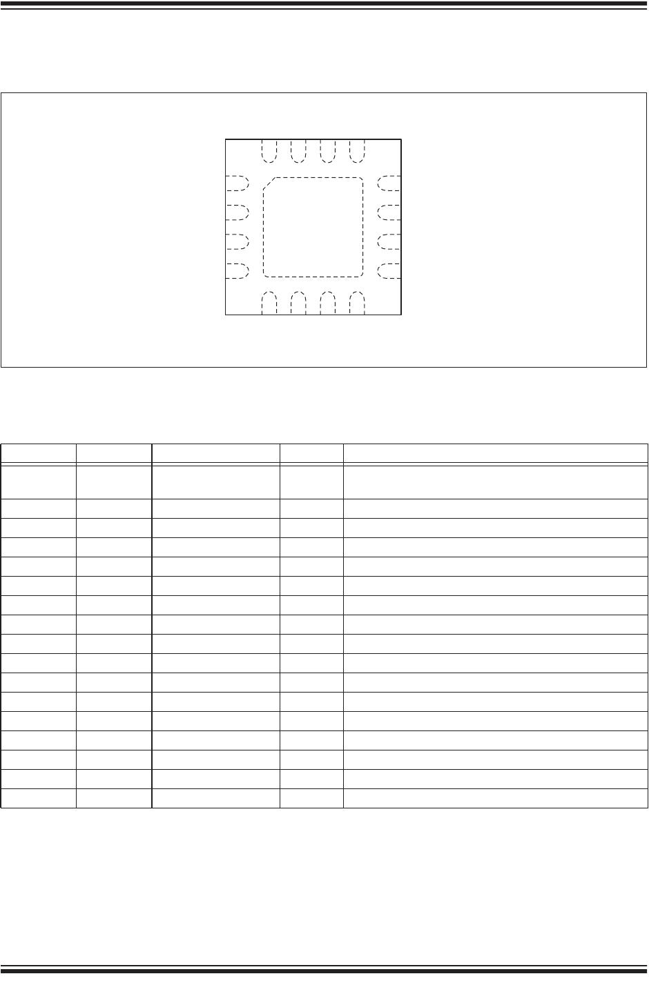
SST12CP12
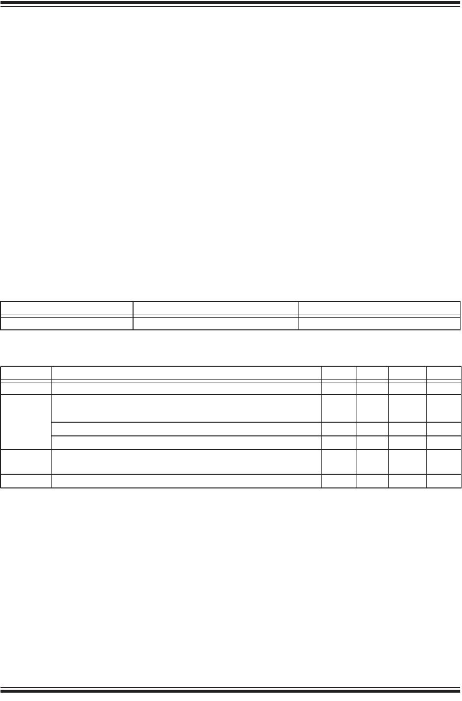
4.0 ELECTRICAL SPECIFICATIONS
The AC and DC specifications for the power amplifier
interface signals. Refer to Table 4-2 for the DC voltage
and current specifications. Refer to Figures 5-1 through
6-5 for the RF performance.
Absolute Maximum Stress Ratings (Applied conditions greater than those listed under “Absolute Maxi-
mum Stress Ratings” may cause permanent damage to the device. This is a stress rating only and func-
tional operation of the device at these conditions or conditions greater than those defined in the operational
sections of this data sheet is not implied. Exposure to absolute maximum stress rating conditions may
affect device reliability.)
Input power to pins 2 and 3 (P
IN
) . . . . . . . . . . . . . . . . . . . . . . . . . . . . . . . . . . . . . . . . . . . . . . . . . . . 5 dBm
Supply Voltage at pins 5, 12, 14, 16 (V
CC
). . . . . . . . . . . . . . . . . . . . . . . . . . . . . . . . . . . . . . . . . . . . . . +6V
Reference voltage to pins 4 (V
REF1
) and pin 7 (V
REF2
) . . . . . . . . . . . . . . . . . . . . . . . . . . . . . . . . . . .+3.5V
DC supply current (I
CC
) . . . . . . . . . . . . . . . . . . . . . . . . . . . . . . . . . . . . . . . . . . . . . . . . . . . . . . . . . 750 mA
Operating Temperature (T
A
) . . . . . . . . . . . . . . . . . . . . . . . . . . . . . . . . . . . . . . . . . . . . . . . . -40ºC to +85ºC
Storage Temperature (T
STG
) . . . . . . . . . . . . . . . . . . . . . . . . . . . . . . . . . . . . . . . . . . . . . . -40ºC to +120ºC
Maximum Junction Temperature (T
J
) . . . . . . . . . . . . . . . . . . . . . . . . . . . . . . . . . . . . . . . . . . . . . . . +150ºC
Surface Mount Solder Reflow Temperature . . . . . . . . . . . . . . . . . . . . . . . . . . . . . . . 260°C for 10 seconds
TABLE 4-1: OPERATING RANGE
Range Ambient Temp V
CC
Industrial -40°C to +85°C 3.0V to 5.0V
TABLE 4-2: DC ELECTRICAL CHARACTERISTICS AT 25ºC
Symbol Parameter Min. Typ Max. Unit
V
CC
Supply Voltage at pins 5, 12, 14, 16 4.0 5.0 5.5 V
I
CC
Average Current at 100% duty cycle
for 802.11g, 28.5 dBm 670 mA
for 802.11b, 28.5 dBm 670 mA
for 256 QAM, 27 dBm 600 mA
I
CQ
Idle current for 802.11g to meet EVM<3% @24.5 dBm, 100% duty
cycle
375 mA
V
REG
Reference Supply 2.90 3.10 3.15 V