Nexperia
74LV1T08
2-input single supply translating AND gate
74LV1T08 All information provided in this document is subject to legal disclaimers. © Nexperia B.V. 2017. All rights reserved.
Product data sheet Rev. 1 — 22 November 2017
4 / 14
9 Limiting values
Table 5. Limiting values
In accordance with the Absolute Maximum Rating System (IEC 60134). Voltages are referenced to GND (ground = 0 V).
Symbol Parameter Conditions Min Max Unit
V
CC
supply voltage -0.5 +7.0 V
V
I
input voltage
[1]
-0.5 +7.0 V
output HIGH or LOW state
[2]
[3]
-0.5 V
CC
+ 0.5 VV
O
output voltage
output in power-off state
[2]
-0.5 4.6 V
I
IK
input clamping current V
I
< 0 V -20 - mA
I
OK
output clamping current V
O
< 0 V or V
O
> V
CC
- ±20 mA
I
O
output current V
O
= 0 V to V
CC
- ±25 mA
I
CC
supply current - 50 mA
I
GND
ground current -50 - mA
T
stg
storage temperature -65 +150 °C
P
tot
total power dissipation T
amb
= -40 °C to +125 °C
[4]
- 250 mW
[1] If the input current ratings are observed, the minimum input voltage ratings may be exceeded.
[2] If the output current ratings are observed, the output voltage ratings may be exceeded.
[3] This value is limited to 7 V maximum.
[4] For TSSOP5 packages: above 75 °C the value of P
tot
derates linearly with 3.3 mW/K.
For X2SON5 package: above 70 °C the value of P
tot
derates linearly with 3.1 mW/K.
10 Recommended operating conditions
Table 6. Recommended operating conditions
Voltages are referenced to GND (ground = 0 V).
Symbol Parameter Conditions Min Typ Max Unit
V
CC
supply voltage 1.6 5.0 5.5 V
V
I
input voltage 0 - 5.5 V
V
O
output voltage output HIGH or LOW state 0 - V
CC
V
T
amb
ambient temperature -40 +25 +125 °C
Δt/ΔV input transition rise and fall rate V
CC
= 1.8 V to 5.0 V - - 20 ns/V
Nexperia
74LV1T08
2-input single supply translating AND gate
74LV1T08 All information provided in this document is subject to legal disclaimers. © Nexperia B.V. 2017. All rights reserved.
Product data sheet Rev. 1 — 22 November 2017
5 / 14
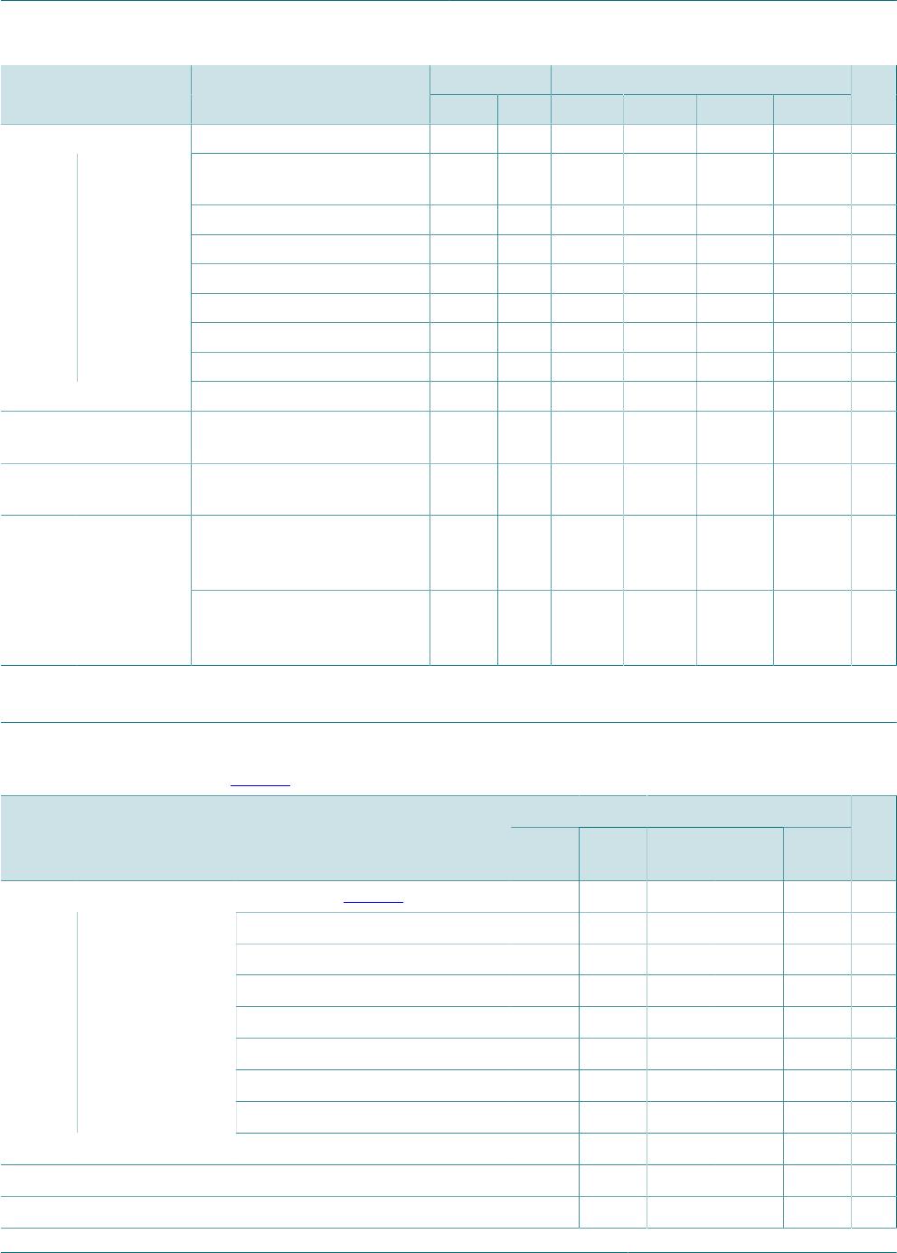
11 Static characteristics
Table 7. Static characteristics
Voltages are referenced to GND (ground = 0 V).
25 °C -40 °C to +85 °C -40 °C to +125 °CSymbol Parameter Conditions
Min Max Min Max Min Max
Unit
V
CC
= 1.65 V to 1.8 V 0.94 - 1.0 - 1.0 - V
V
CC
= 2.0 V 0.99 - 1.03 - 1.03 - V
V
CC
= 2.25 V to 2.5 V 1.135 - 1.18 - 1.18 - V
V
CC
= 2.75 V 1.21 - 1.23 - 1.23 - V
V
CC
= 3.0 V to 3.3 V 1.35 - 1.37 - 1.37 - V
V
CC
= 3.6 V 1.47 - 1.48 - 1.48 - V
V
CC
= 4.5 V to 5.0 V 2.02 - 2.03 - 2.03 - V
V
IH
HIGH-level
input voltage
V
CC
= 5.5 V 2.10 - 2.11 - 2.11 - V
V
CC
= 1.65 V to 2.0 V - 0.58 - 0.55 - 0.55 V
V
CC
= 2.25 V to 2.75 V - 0.75 - 0.71 - 0.71 V
V
CC
= 3.0 V to 3.6 V - 0.80 - 0.65 - 0.65 V
V
IL
LOW-level
input voltage
V
CC
= 4.5 V to 5.5 V - 0.80 - 0.80 - 0.80 V
V
I
= V
IH
or V
IL
;
V
CC
= 1.65 V to 5.5 V;
I
O
= -20 μA
V
CC
-0.1 - V
CC
-0.1 - V
CC
-0.1 - V
V
CC
= 1.65 V; I
O
= -2 mA 1.28 - 1.21 - 1.21 - V
V
CC
= 1.8 V; I
O
= -2 mA 1.5 - 1.45 - 1.45 - V
V
CC
= 2.3 V; I
O
= -2.3 mA 2.0 - 2.0 - 2.0 - V
V
CC
= 2.3 V; I
O
= -3 mA 2.0 - 1.93 - 1.93 - V
V
CC
= 2.5 V; I
O
= -3 mA 2.25 - 2.15 - 2.15 - V
V
CC
= 3.0 V; I
O
= -3 mA 2.78 - 2.7 - 2.7 - V
V
CC
= 3.0 V; I
O
= -5.5 mA 2.6 - 2.49 - 2.49 - V
V
CC
= 3.3 V; I
O
= -5.5 mA 2.9 - 2.8 - 2.8 - V
V
CC
= 4.5 V; I
O
= -4 mA 4.2 - 4.1 - 4.1 - V
V
CC
= 4.5 V; I
O
= -8 mA 4.1 - 3.95 - 3.95 - V
V
OH
HIGH-level
output voltage
V
CC
= 5.0 V; I
O
= -8 mA 4.6 - 4.5 - 4.5 - V
Nexperia
74LV1T08
2-input single supply translating AND gate
74LV1T08 All information provided in this document is subject to legal disclaimers. © Nexperia B.V. 2017. All rights reserved.
Product data sheet Rev. 1 — 22 November 2017
6 / 14
25 °C -40 °C to +85 °C -40 °C to +125 °CSymbol Parameter Conditions
Min Max Min Max Min Max
Unit
V
I
= V
IH
or V
IL
V
CC
= 1.65 V to 5.5 V;
I
O
= 20 μA
- 0.1 - 0.1 - 0.1 V
V
CC
= 1.65 V; I
O
= 2 mA - 0.2 - 0.25 - 0.25 V
V
CC
= 2.3 V; I
O
= 2.3 mA - 0.1 - 0.15 - 0.15 V
V
CC
= 2.3 V; I
O
= 3 mA - 0.15 - 0.2 - 0.2 V
V
CC
= 3.0 V; I
O
= 3 mA - 0.1 - 0.15 - 0.15 V
V
CC
= 3.0 V; I
O
= 5.5 mA - 0.2 - 0.252 - 0.252 V
V
CC
= 4.5 V; I
O
= 4 mA - 0.15 - 0.2 - 0.2 V
V
OL
LOW-level
output voltage
V
CC
= 4.5 V; I
O
= 8 mA - 0.3 - 0.35 - 0.35 V
I
I
input leakage
current
V
I
= V
CC
or GND;
V
CC
= 0 V to 5.5 V
- ±0.1 - ±1 - ±1 μA
I
CC
supply current V
I
= V
CC
or GND; I
O
= 0 A;
V
CC
= 1.8 V, 2.5 V, 3.3 V, 5.0 V
- 1 - 10 - 10 μA
per input pin; V
CC
= 1.8 V;
V
I
= 0.3 V or 1.1 V; I
O
= 0 A;
other pins at V
CC
or GND
- 10 - 10 - 10 μAΔI
CC
additional
supply current
per input pin; V
CC
= 5.5 V;
V
I
= 0.3 V or 3.4 V; I
O
= 0 A;
other pins at V
CC
or GND
- 1.35 - 1.5 - 1.5 mA
12 Dynamic characteristics
Table 8. Dynamic characteristics
GND = 0 V. For test circuit, see Figure 7.
-40 °C to +125 °CSymbol Parameter Conditions
Min Typ
25 °C
Max
25 °C
Max
85 °C
Max
125 °C
Unit
A, B to Y; see Figure 6
[1]
V
CC
= 1.8 V; C
L
= 15 pF - 6.5 9.7 10.9 11.7 ns
V
CC
= 1.8 V; C
L
= 30 pF - 7.6 10.9 12.4 13.4 ns
V
CC
= 2.5 V; C
L
= 15 pF - 4.6 6.6 7.6 8.2 ns
V
CC
= 2.5 V; C
L
= 30 pF - 5.3 7.5 8.6 9.2 ns
V
CC
= 3.3 V; C
L
= 15 pF - 3.8 5.4 6.1 6.5 ns
V
CC
= 3.3 V; C
L
= 30 pF - 4.4 6.1 6.8 7.3 ns
V
CC
= 5.0 V; C
L
= 15 pF - 3.2 4.1 4.5 4.7 ns
t
pd
propagation delay
V
CC
= 5.0 V; C
L
= 30 pF - 3.6 4.6 5.1 5.4 ns
C
I
input capacitance V
I
= V
CC
or GND; V
CC
= 3.3 V - 1.5 10 10 10 pF
C
O
output capacitance V
O
= V
CC
or GND; V
CC
= 3.3 V - 2.5 - - - pF

74LV1T08GXH

Mfr. #:
Manufacturer:
Nexperia
Description:
Translation - Voltage Levels 2-input single supply translating AND gate - SOT1226 X2SON5
Lifecycle:
New from this manufacturer.
Delivery:
DHL FedEx Ups TNT EMS
Payment:
T/T Paypal Visa MoneyGram Western Union

Products related to this Datasheet