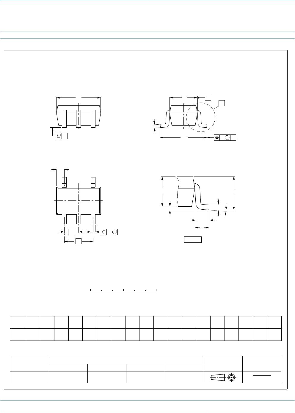
Nexperia
74LV1T08
2-input single supply translating AND gate
74LV1T08 All information provided in this document is subject to legal disclaimers. © Nexperia B.V. 2017. All rights reserved.
Product data sheet Rev. 1 — 22 November 2017
8 / 14
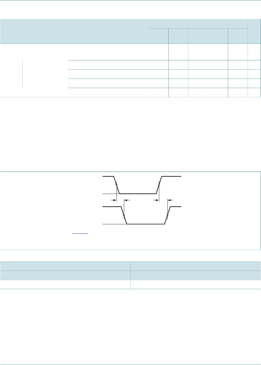
aaa-027728
V
M
V
M
V
M
V
M
t
f
10 % 10 %
90 %
90 %90 %
10 % 10 %
V
I
0 V
V
I
negative
pulse
positive
pulse
0 V
90 %
t
W
t
r
t
r
t
f
t
W
G
DUT
V
CC
V
EXT
V
I
V
O
R
T
R
L
C
L
Test data is given in Table 10.
Definitions test circuit:
R
T
= Termination resistance should be equal to output impedance Z
o
of the pulse generator
C
L
= Load capacitance including jig and probe capacitance
R
L
= Load resistance
V
EXT
= External voltage for measuring switching times
Figure 7. Test circuit for measuring switching times
Table 10. Test data
Supply voltage Input Load V
EXT
V
CC
V
I
Δt/ΔV
[1]
f
max
C
L
R
L
t
PLH
, t
PHL
t
PZH
, t
PHZ
t
PZL
, t
PLZ
1.8 V V
CC
≤ 1.0 ns/V 15 MHz 15 pF, 30 pF 1MΩ GND GND V
CC
2.5 V V
CC
≤ 1.0 ns/V 25 MHz 15 pF, 30 pF 1MΩ GND GND V
CC
3.3 V 3 V ≤ 1.0 ns/V 50 MHz 15 pF, 30 pF 1MΩ GND GND V
CC
5.0 V 3 V ≤ 1.0 ns/V 50 MHz 15 pF, 30 pF 1MΩ GND GND V
CC
[1] dV/dt ≥ 1.0 V/ns