NXP Semiconductors
BGU8062
low-noise high-linearity amplifier
BGU8062 All information provided in this document is subject to legal disclaimers. © NXP Semiconductors N.V. 2017. All rights reserved.
Product data sheet Rev. 2 — 24 January 2017
4 / 18
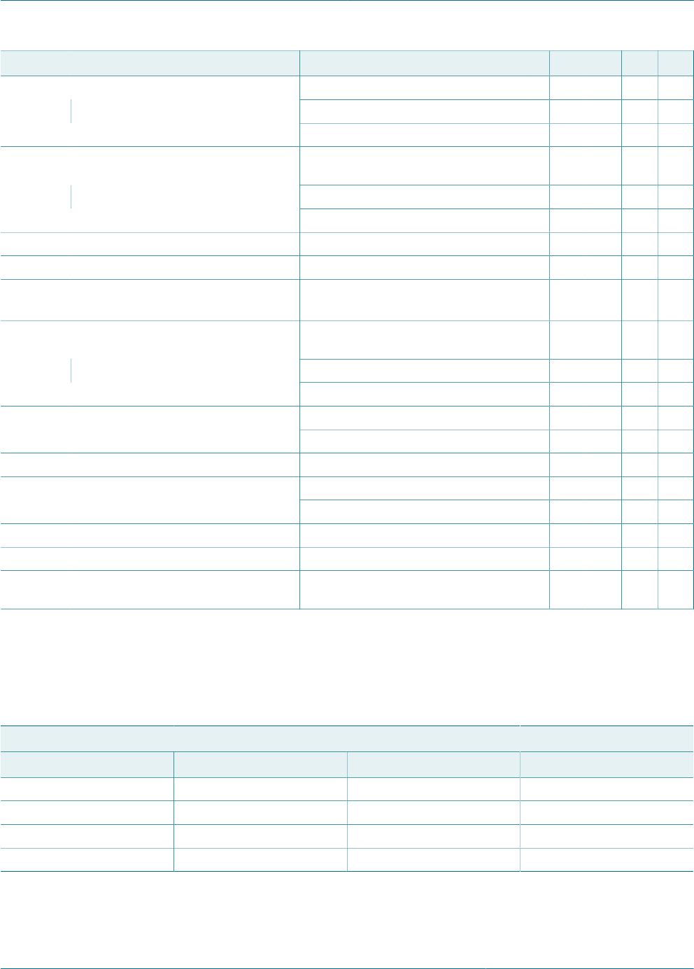
8 Limiting values
Table 4. Limiting values
In accordance with the Absolute Maximum Rating System (IEC 60134). See Section 16.3 "Disclaimers", paragraph "Limiting
values".
Symbol Parameter Conditions Min Max Unit
V
CC
supply voltage - 6 V
V
I(CTRL1)
input voltage on pin CTRL1 - 3.6 V
V
I(CTRL2)
input voltage on pin CTRL2 - 3.6 V
P
i(RF)CW
continuous waveform RF input power - 20 dBm
T
stg
storage temperature -40 +150 °C
T
j
junction temperature - 150 °C
P power dissipation T
case
≤ 125 °C
[1]
- 510 mW
Human Body Model (HBM); according to
ANSI/ESDA/JEDEC standard JS-001-2010
- 2.0 kVV
ESD
electrostatic discharge voltage
Charged Device Model (CDM); according
to JEDEC standard 22-C101B
- 1.0 kV
[1] Case is ground solder pad.
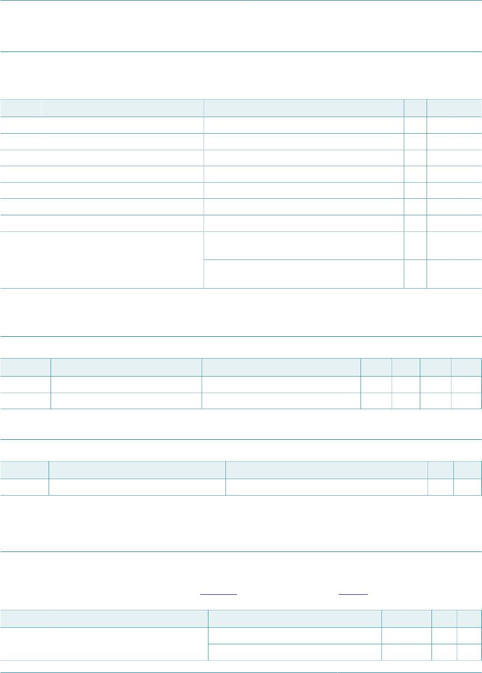
9 Recommended operating conditions
Table 5. Characteristics
Symbol Parameter Conditions Min Typ Max Unit
V
CC
supply voltage 4.75 5 5.25 V
Z
0
characteristic impedance - 50 - Ω
10 Thermal characteristics
Table 6. Thermal characteristics
Symbol Parameter Conditions Typ Unit
R
th(j-case)
thermal resistance from junction to case
[1]
[2]
55 K/W
[1] Case is ground solder pad.
[2] Thermal resistance measured using infrared measurement technique, device mounted on application board and placed in still air.
11 Characteristics
Table 7. Characteristics
f = 1900 MHz; V
CC
= 5 V; T
amb
= 25 °C; input and output 50 Ω; unless otherwise specified. All RF parameters are measured
on an application board with the circuit as shown in Figure 29 and components listed in Table 9 implemented. This board is
optimized for f = 1900 MHz.
Symbol Parameter Conditions Min Typ Max Unit
LNA enable; bypass off - 70 85 mAI
CC
supply current
LNA disable; bypass on - 3 5 mA