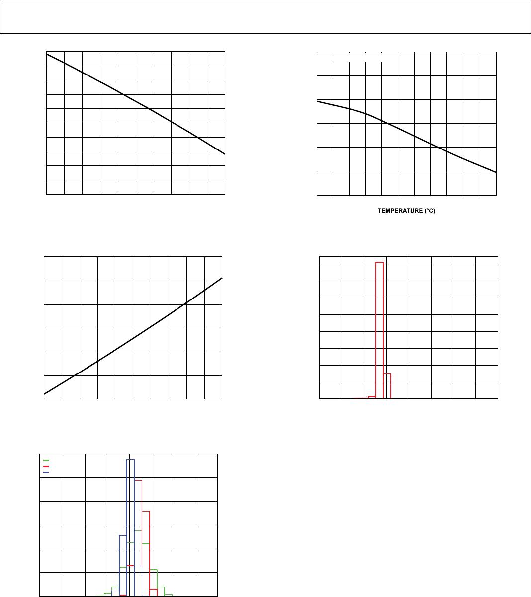
Data Sheet AD8417
–500
–450
–400
–350
–300
–250
–200
–150
–100
–50
0
0 1 2 3 4 5 6 7 8 9 10
OUTPUT VOLTAGE RANGE FROM
POSITIVE RAIL (mV)
OUTPUT SOURCE CURRENT (mA)
11882-021
Figure 21. Output Voltage Range from Positive Rail vs. Output Source Current
0
50
100
150
200
250
300
0 1 2 3 4 5 6 7 8 9 10
OUTPUT VOLTAGE RANGE FROM
POSITIVE RAIL (mV)
OUTPUT SINK CURRENT (mA)
11882-022
Figure 22. Output Voltage Range from Ground vs. Output Sink Current
–400
–300
–200
–100
0
100
200
300 400
0
300
600
900
1200
1500
1800
V
OSI
WITH V
CC
= 5.0V (µV)
–40°C
+25°C
+125°C
HITS
11882-023
Figure 23. Offset Voltage Distribution
–0.15
–0.10
–0.05
0
0.05
0.10
0.15
–40 –25 –10
5 20 35 50 65 80 95 110 125
CMRR (µV/V)
NORMALIZED
A
T 25°C
11882-024
Figure 24. CMRR vs. Temperature
–8
–6
–4
–2
0
2
4
6 8
0
300
600
900
1200
1500
1800
2100
2400
GAIN ERROR DRIFT (ppm/°C)
HITS
11882-125
Figure 25. Gain Error Drift Distribution
Rev. B | Page 9 of 16
AD8417 Data Sheet
Rev. B | Page 10 of 16
THEORY OF OPERATION
The AD8417 is a single-supply, zero drift, difference amplifier
that uses a unique architecture to accurately amplify small
differential current shunt voltages in the presence of rapidly
changing common-mode voltages.
In typical applications, the AD8417 measures current by
amplifying the voltage across a shunt resistor connected to its
inputs by a gain of 60 V/V (see Figure 26).
The AD8417 design provides excellent common-mode rejection,
even with PWM common-mode inputs that can change at very
fast rates, for example, 1 V/ns. The AD8417 contains patented
technology to eliminate the negative effects of such fast
changing external common-mode variations.
The AD8417 features an input offset drift of less than 0.4 μVC.
This performance is achieved through a novel zero drift
architecture that does not compromise bandwidth, which is
typically rated at 250 kHz.
The reference inputs, V
REF
1 and V
REF
2, are tied through 100 kΩ
resistors to the positive input of the main amplifier, which allows
the output offset to be adjusted anywhere in the output operating
range. The gain is 1 V/V from the reference pins to the output
when the reference pins are used in parallel. When the pins are
used to divide the supply, the gain is 0.5 V/V.
The AD8417 offers breakthrough performance without
compromising any of the robust application needs typical of
solenoid or motor control. The ability to reject PWM input
common-mode voltages and the zero drift architecture
providing low offset and offset drift allows the AD8417 to
deliver total accuracy for these demanding applications.
+
I
SHUNT
G = 60
V
CM
= –2V TO +70
V
V
S
= 2.7V TO 5.5
V
V
REF
1
V
REF
2
OUT
0V
V
S
V
S
/2
V
OUT
I
SHUNT
EMI
FILTER
EMI
FILTER
V
CM
0V
70V
AD8417
V
S
+IN
–IN
GND
–50A
50A
R
SHUNT
11882-225
Figure 26. Typical Application
Data Sheet AD8417
OUTPUT OFFSET ADJUSTMENT
The output of the AD8417 can be adjusted for unidirectional or
bidirectional operation.
UNIDIRECTIONAL OPERATION
Unidirectional operation allows the AD8417 to measure currents
through a resistive shunt in one direction. The basic modes for
unidirectional operation are ground referenced output mode
and V
S
referenced output mode.
For unidirectional operation, the output can be set at the negative
rail (near ground) or at the positive rail (near V
S
) when the
differential input is 0 V. The output moves to the opposite rail
when a correct polarity differential input voltage is applied. The
required polarity of the differential input depends on the output
voltage setting. If the output is set at the positive rail, the input
polarity must be negative to decrease the output. If the output is
set at ground, the polarity must be positive to increase the output.
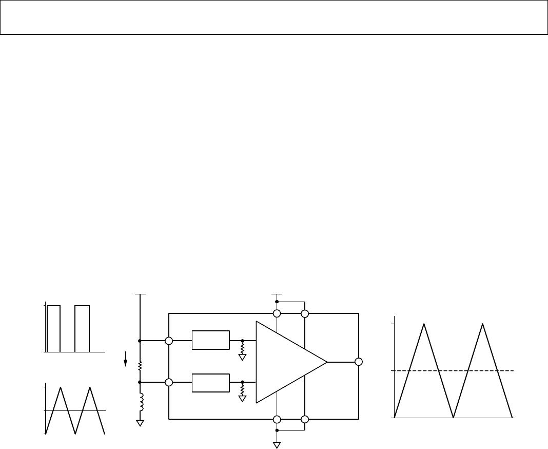
Ground Referenced Output Mode
When using the AD8417 in ground referenced output mode, both
referenced inputs are tied to ground, which causes the output to sit
at the negative rail when there are zero differential volts at the input
(see Figure 27).
+
R1
OUT
GND
V
S
V
REF
1
V
REF
2
AD8417
R2
R3
R4
–IN
+IN
11882-025
Figure 27. Ground Referenced Output
V
S
Referenced Output Mode
V
S
referenced output mode is set when both reference pins are tied
to the positive supply. It is typically used when the diagnostic
scheme requires detection of the amplifier and the wiring before
power is applied to the load (see Figure 28).
+
R1
OUT
GND
V
S
V
REF
1
V
REF
2
AD8417
R2
R3
R4
–IN
+IN
11882-026
Figure 28. V
S
Referenced Output
BIDIRECTIONAL OPERATION
Bidirectional operation allows the AD8417 to measure currents
through a resistive shunt in two directions.
In this case, the output is set anywhere within the output range.
Typically, it is set at half-scale for equal range in both directions.
In some cases, however, it is set at a voltage other than half scale
when the bidirectional current is nonsymmetrical.
Adjusting the output is accomplished by applying voltage(s) to
the referenced inputs. V
REF
1 and V
REF
2 are tied to internal
resistors that connect to an internal offset node. There is no
operational difference between the pins.
Rev. B | Page 11 of 16

AD8417BRMZ

Mfr. #:
Manufacturer:
Analog Devices Inc.
Description:
Current Sense Amplifiers DMOS CSAmp G=60 BiDir 0 Drift
Lifecycle:
New from this manufacturer.
Delivery:
DHL FedEx Ups TNT EMS
Payment:
T/T Paypal Visa MoneyGram Western Union