Data Sheet AD8417
SPECIFICATIONS
T
A
= 40°C to +125°C (operating temperature range) for the AD8417WB, T
A
= −40°C to +150°C for the AD8417WH, V
S
= 5 V, unless
otherwise noted.
Table 2.
Parameter Test Conditions/Comments Min Typ Max Unit
GAIN
Initial 60 V/V
Error Over Temperature Specified temperature range ±0.3 %
Gain vs. Temperature 10 +10 ppm/°C
VOLTAGE OFFSET
Offset Voltage, Referred to the Input (RTI) 25°C ±200 µV
Over Temperature (RTI) Specified temperature range ±400 µV
Offset Drift 0.4 +0.1 +0.4 µV/°C
INPUT
Input Bias Current 130 µA
Input Voltage Range Common mode, continuous −2 +70 V
Common-Mode Rejection Ratio (CMRR) Specified temperature range, f = dc 90 100 dB
f = dc to 10 kHz 86 dB
OUTPUT
Output Voltage Range
R
L
= 25 kΩ
0.045
S
V
Output Resistance 2
DYNAMIC RESPONSE
Small Signal −3 dB Bandwidth 250 kHz
Slew Rate 1 V/µs
NOISE
0.1 Hz to 10 Hz (RTI) 2.3 µV p-p
Spectral Density, 1 kHz (RTI) 110 nV/Hz
OFFSET ADJUSTMENT
Ratiometric Accuracy
1
Divider to supplies 0.499 0.501 V/V
Accuracy, Referred to the Output (RTO) Voltage applied to V
REF
1 and V
REF
2 in parallel ±1 mV/V
Output Offset Adjustment Range V
S
= 5 V 0.045 V
S
− 0.035 V
POWER SUPPLY
Operating Range 2.7 5.5 V
Quiescent Current Over Temperature V
OUT
= 0.1 V dc
AD8417WB 4.1 mA
AD8417WH 4.2 mA
Power Supply Rejection Ratio 80 dB
Temperature Range
For Specified Performance Operating temperature range
AD8417WB 40 +125 °C
AD8417WH 40 +150 °C
1
The offset adjustment is ratiometric to the power supply when V
REF
1 and V
REF
2 are used as a divider between the supplies.
Rev. B | Page 3 of 16
AD8417 Data Sheet
ABSOLUTE MAXIMUM RATINGS
Table 3.
Parameter Rating
Supply Voltage 6 V
Input Voltage Range
Continuous 2 V to +70 V
Survival 4 V to +85 V
Differential Input Survival ±5.5 V
Reverse Supply Voltage 0.3 V
ESD Human Body Model (HBM) ±2000 V
Operating Temperature Range
AD8417WB 40°C to +125°C
AD8417WH 40°C to +150°C
Storage Temperature Range 65°C to +150°C
Output Short-Circuit Duration Indefinite
Stresses at or above those listed under Absolute Maximum
Ratings may cause permanent damage to the product. This is a
stress rating only; functional operation of the product at these
or any other conditions above those indicated in the operational
section of this specification is not implied. Operation beyond
the maximum operating conditions for extended periods may
affect product reliability.
ESD CAUTION
Rev. B | Page 4 of 16
Data Sheet AD8417
Rev. B | Page 5 of 16
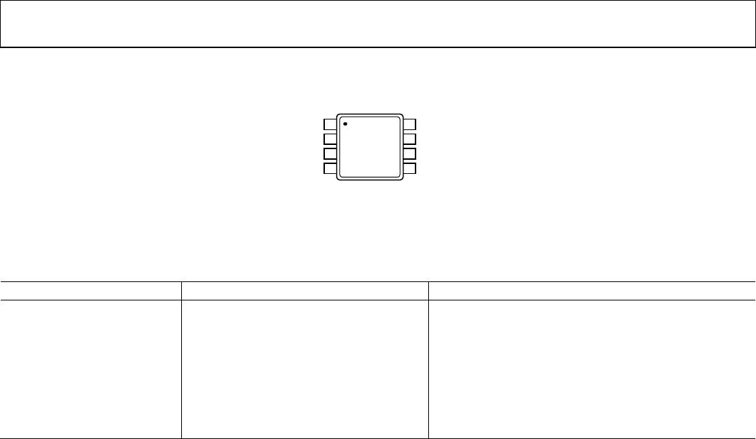
PIN CONFIGURATION AND FUNCTION DESCRIPTIONS
NC = NO CONNECT. DO NOT
CONNECT TO THIS PIN.
–IN
1
GND
2
V
REF
2
3
NC
4
+IN
8
V
REF
1
7
V
S
6
OUT
5
AD8417
TOP VIEW
(Not to Scale)
11882-002
Figure 2. Pin Configuration
Table 4. Pin Function Descriptions
Pin No. Mnemonic Description
1 −IN Negative Input.
2 GND Ground.
3 V
REF
2 Reference Input 2.
4 NC No Connect. Do not connect to this pin.
5 OUT Output.
6 V
S
Supply.
7 V
REF
1 Reference Input 1.
8 +IN Positive Input.

AD8417BRMZ

Mfr. #:
Manufacturer:
Analog Devices Inc.
Description:
Current Sense Amplifiers DMOS CSAmp G=60 BiDir 0 Drift
Lifecycle:
New from this manufacturer.
Delivery:
DHL FedEx Ups TNT EMS
Payment:
T/T Paypal Visa MoneyGram Western Union