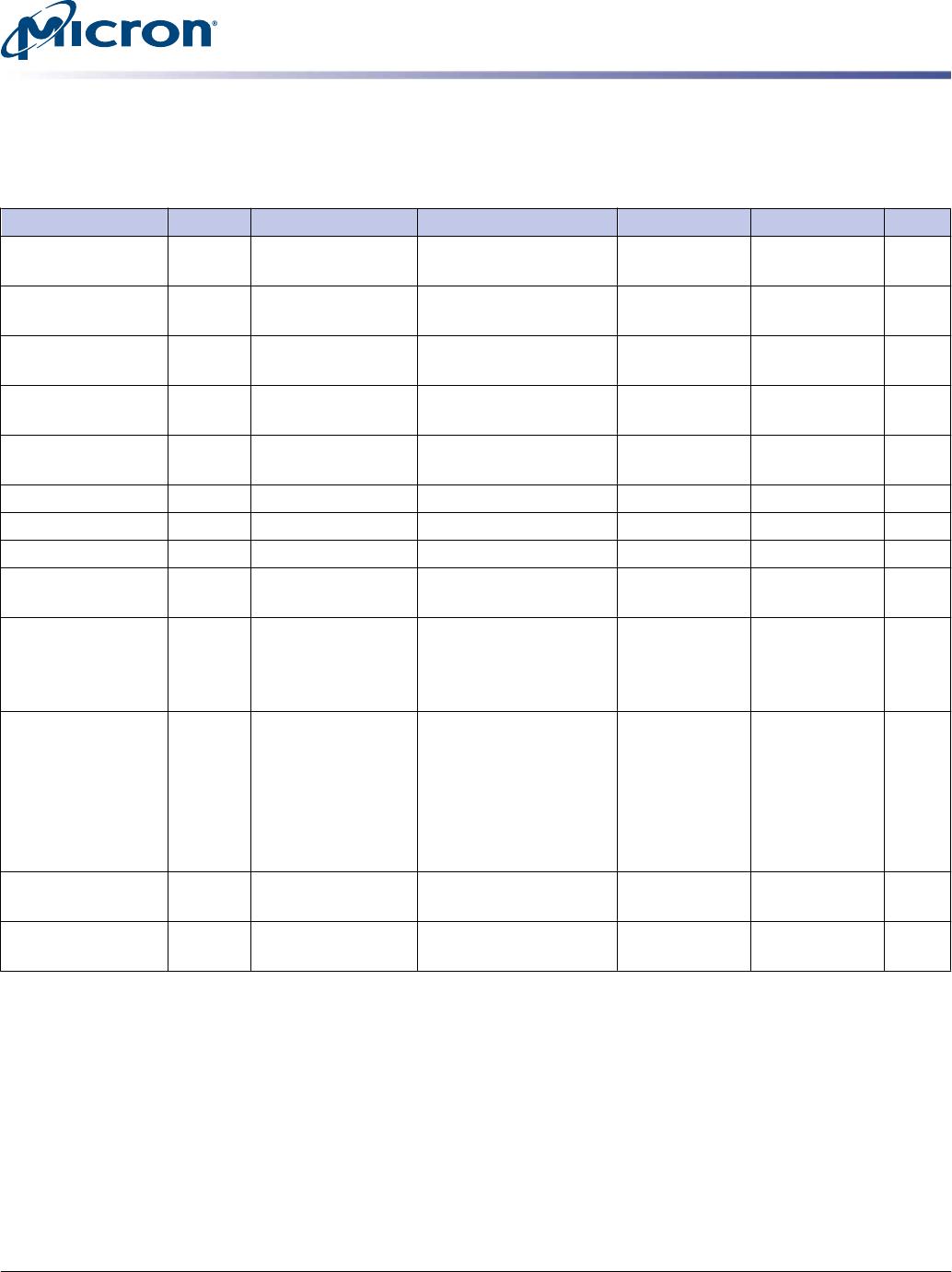
IDD Specifications
Table 8: DDR2 I
CDD
Specifications and Conditions – 8GB (Die Revision C)
Values shown for MT47H1G4 DDR2 SDRAM only and are computed from values specified in the 4Gb TwinDie (1 Gig x 4)
component data sheet
Parameter
Combined
Symbol
-80E/
-800 -667 Units
Operating one bank active-precharge current:
t
CK =
t
CK (I
DD
),
t
RC =
t
RC
(I
DD
),
t
RAS =
t
RAS MIN (I
DD
); CKE is HIGH, S# is HIGH between valid commands;
Address bus inputs are switching; Data bus inputs are switching
I
CDD0
1656 1566 mA
Operating one bank active-read-precharge current: I
OUT
= 0mA; BL = 4,
CL = CL (I
DD
), AL = 0;
t
CK =
t
CK (I
DD
),
t
RC =
t
RC (I
DD
),
t
RAS =
t
RAS MIN (I
DD
),
t
RCD =
t
RCD (I
DD
); CKE is HIGH, S# is HIGH between valid commands; Address
bus inputs are switching; Data pattern is same as I
DD4W
I
CDD1
1926 1836 mA
Precharge power-down current: All device banks idle;
t
CK =
t
CK (I
DD
); CKE is
LOW; Other control and address bus inputs are stable; Data bus inputs are
floating
I
CDD2P
432 432 mA
Precharge quiet standby current: All device banks idle;
t
CK =
t
CK (I
DD
); CKE
is HIGH, S# is HIGH; Other control and address bus inputs are stable; Data bus
inputs are floating
I
CDD2Q
846 756 mA
Precharge standby current: All device banks idle;
t
CK =
t
CK (I
DD
); CKE is
HIGH, S# is HIGH; Other control and address bus inputs are switching; Data bus
inputs are switching
I
CDD2N
936 846 mA
Active power-down current: All device banks open;
t
CK =
t
CK (I
DD
); CKE is LOW; Other control and address bus inputs
are stable; Data bus inputs are floating
Fast PDN exit
MR[12] = 0
I
CDD3P
756 666 mA
Slow PDN exit
MR[12] = 1
468 468
Active standby current: All device banks open;
t
CK =
t
CK (I
DD
),
t
RAS =
t
RAS
MAX (I
DD
),
t
RP =
t
RP (I
DD
); CKE is HIGH, S# is HIGH between valid commands;
Other control and address bus inputs are switching; Data bus inputs are switching
I
CDD3N
1116 1026 mA
Operating burst write current: All device banks open; Continuous burst
writes; BL = 4, CL = CL (I
DD
), AL = 0;
t
CK =
t
CK (I
DD
),
t
RAS =
t
RAS MAX (I
DD
),
t
RP =
t
RP (I
DD
); CKE is HIGH, S# is HIGH between valid commands; Address bus inputs
are switching; Data bus inputs are switching
I
CDD4W
2916 2556 mA
Operating burst read current: All device banks open; Continuous burst read,
I
OUT
= 0mA; BL = 4, CL = CL (I
DD
), AL = 0;
t
CK =
t
CK (I
DD
),
t
RAS =
t
RAS MAX (I
DD
),
t
RP =
t
RP (I
DD
); CKE is HIGH, S# is HIGH between valid commands; Address bus
inputs are switching; Data bus inputs are switching
I
CDD4R
2916 2556 mA
Burst refresh current:
t
CK =
t
CK (I
DD
); REFRESH command at every
t
RFC (I
DD
)
interval; CKE is HIGH, S# is HIGH between valid commands; Other control and
address bus inputs are switching; Data bus inputs are switching
I
CDD5
3546 3186 mA
Self refresh current: CK and CK# at 0V; CKE ≤ 0.2V; Other control and ad-
dress bus inputs are floating; Data bus inputs are floating
I
CDD6
432 432 mA
8GB (x72, ECC, DR) 240-Pin DDR2 VLP RDIMM
IDD Specifications
PDF: 09005aef845bf514
hvzs36c1gx72pz.pdf - Rev. A 5/11 EN
10
Micron Technology, Inc. reserves the right to change products or specifications without notice.
© 2011 Micron Technology, Inc. All rights reserved.