2
LTC1040
1040fa
ORDER PART
NUMBER
LTC1040CN
LTC1040CSW
LTC1040MJ
LTC1040CJ
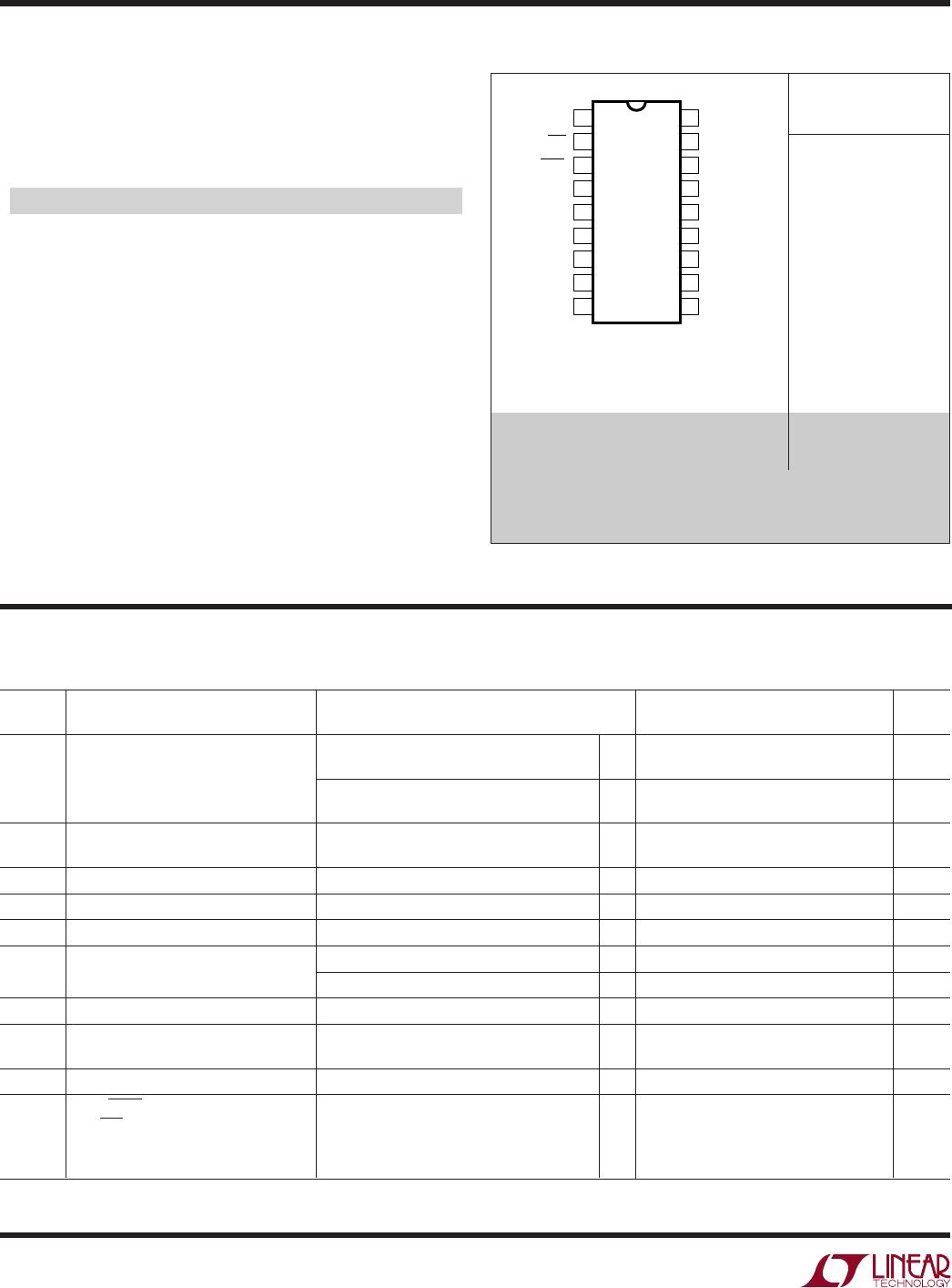
N PACKAGE
18-LEAD PDIP
TOP VIEW
1
2
3
4
5
6
7
8
9
18
17
16
15
14
13
12
11
10
STROBE
ON/OFF
A + B
A
OUT
A1
+
A1
–
A2
+
A2
–
GND
V
+
V
P-P
OSC
B
OUT
B1
+
B1
–
B2
+
B2
–
V
–
J PACKAGE
18-LEAD CERDIP
T
JMAX
= 150°C, θ
JA
= 80°C/W
SW PACKAGE
18-LEAD PLASTIC SO WIDE
T
JMAX
= 110°C, θ
JA
= 120°C/W (N)
T
JMAX
= 125°C, θ
JA
= 85°C/W (SW)
Total Supply Voltage (V
+
to V
–
) ............................... 18V
lnput Voltage ........................ (V
+
+ 0.3V) to (V
–
– 0.3V)
Operating Temperature Range
LTC1040C..................................... –40°C ≤ T
A
≤ 85°C
LTC1040M (OBSOLETE) .................... –55°C to 125°C
Storage Temperature Range ................. –55°C to 150°C
Lead Temperature (Soldering, 10 sec)..................300°C
Output Short-Circuit Duration.......................Continuous
ABSOLUTE AXI U RATI GS
WWWU
PACKAGE/ORDER I FOR ATIO
UU
W
(Note 1)
ELECTRICAL CHARACTERISTICS
The ● denotes the specifications which apply over the full operating
temperature range, otherwise specifications are at T
A
= 25°C. Test conditions: V
+
= 5V, V
–
= –5V, unless otherwise noted.
LTC1040M/LTC1040C
SYMBOL PARAMETER CONDITIONS MIN TYP MAX UNITS
V
OS
Offset Voltage (Note 2) Split Supplies ±2.8V to ±6V ● ±0.3 ± 0.75 mV
Single Supply (V
–
= GND) 2.8V to 6V
Split Supplies ±6V to ±8V ● ±1 ±4.5 mV
Single Supply (V
–
= GND) 6V to 15V
Tracking Error Between Split Supplies ±2.8V to ±8V ● 0.05 0.1 %
Input Pairs (Notes 2 and 3) Single Supplies (V
–
= GND) 2.8 to 16V
I
BIAS
Input Bias Current OSC = GND ±0.3 nA
R
IN
Average Input Resistance f
S
= 1kHz (Note 4) ● 20 30 MΩ
CMR Common Mode Range ● V
–
V
+
V
PSR Power Supply Range Split Supplies ● ±2.8 ±8 V
Single Supplies (V
–
= GND) ● 2.8 16 V
I
S(ON)
Power Supply ON Current (Note 5) V
+
= 5V, V
P-P
On ● 1.2 3 mA
I
S(OFF)
Power Supply OFF Current (Note 5) V
+
= 5V, V
P-P
Off LTC1040C ● 0.001 0.5 µA
LTC1040M ● 0.001 5 µA
t
D
Response Time (Note 6) 60 80 100 µs
A, B, A + B and
ON/OFF Outputs (Note 7)
V
OH
Logic “1” Output Voltage V
+
= 4.75V, l
OUT
= –360µA ● 2.4 4.4 V
V
OL
Logic “0” Output Voltage V
+
= 4.75V, l
OUT
= 1.6mA ● 0.25 0.4 V
OBSOLETE PACKAGE
Consider the N18 Package as an Alternate Source
Consult LTC Marketing for parts specified with wider operating temperature ranges.