7
LTC1040
1040fa
1A
100mV
APPLICATIO S I FOR ATIO
WUUU
Offset Voltage Error
The errors due to offset, common mode, power supply
variation, gain and temperature are all included in the
offset voltage specification. This makes it easy to compute
the error when using the LTC1040.
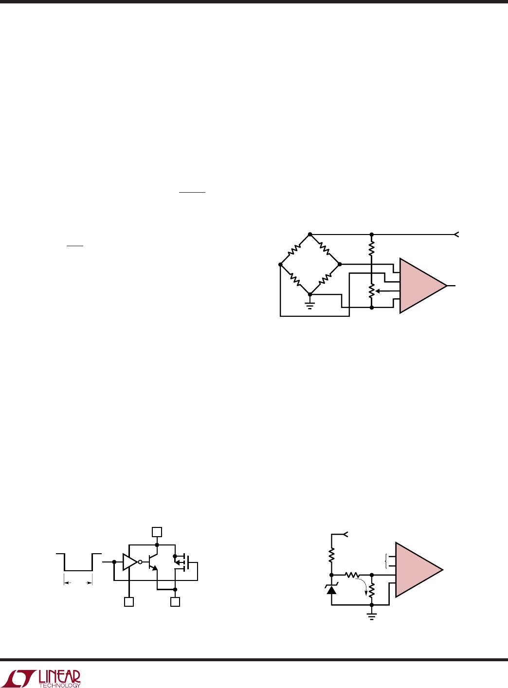
Example: error computation for Figure 4.
Assume: 2.8V ≤ V
S
≤ 6V.
Then total worst-case error is:
Note: If source resistance exceeds 10k, bypass
capacitors should be used and the associated errors must
be included.
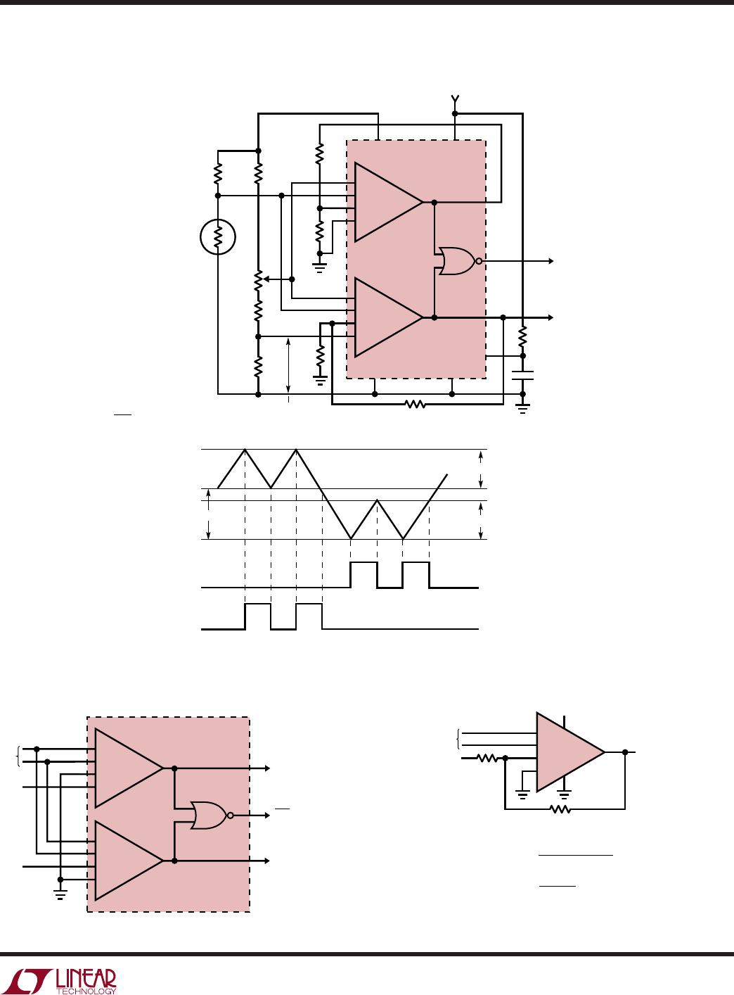
Pulsed Power (V
P-P
) Output
It is often desirable to use comparators with resistive
networks such as bridges. Because of the extremely low
power consumption of the LTC1040, the power consumed
by these resistive networks can far exceed that of the
device itself.
At low sample rates the LTC1040 spends most of its time
off. To take advantage of this, a pulsed power (V
P-P
) output
is provided. V
P-P
is switched to V
+
when the comparator
is on and to a high impedance (open circuit) when the
comparator is off. The ON time is nominally 80µs.
Figure 5 shows the V
P-P
output circuit.
The V
P-P
output voltage is not precise (see V
P-P
Output
Voltage versus Load Current curve). There are two ways
V
P-P
can be used to power external networks without
excessive errors: (1) ratiometric networks and (2) fast
settling references.
In a ratiometric network, the inputs are all proportional to
V
P-P
(see Figure 6). Consequently, for small changes, the
absolute value of V
P-P
does not affect accuracy.
It is critical that the inputs to the LTC1040 completely
settle within 4µs of the start of the comparison cycle and
that they do not change during the 80µs ON time. When
driving resistive networks with V
P-P
, capacitive loading on
the network should be minimized to meet the 4µs settling
time requirement. It is not recommended that V
P-P
be used
to drive networks with source impedances, as seen by the
inputs, of greater than 10kΩ.
In applications where an absolute reference is required,
the V
P-P
output can be used to drive a fast settling
reference. The LT1009 2.5V reference, ideal in this
application, settles in approximately 2µs (see Figure 7).
The current through R1 must be large enough to supply
the LT1009 minimum bias current (≈1mA) and the load
current, I
L
.
LTC1040 • AI05
80µs
COMPARATOR ON TIME
18
V
+
917
GND
Q1 P1
V
P-P
Figure 7. Driving Reference with V
P-P
Output
Figure 6. Ratiometric Network Driven by
V
P-P
Figure 5. V
P-P
Output Switch
= ±6mA
I
L (ERROR)
= ± (100mV • 0.001 + 0.5mV) •
↑↑
Tracking Error V
OS
I
L (ERROR)
% = • 100 = ± 0.6%.
6mA
1A
V
IN
V
TRIP
OUTPUT
V
P-P
OUTPUT
LTC1040 • AI06
–
–+
–
+
+
1/2
LTC1040
V
IN
I
L
V
P-P
OUTPUT
LTC1040 • AI07
–
–
+
+
1/2
LTC1040
R2
R3
LT1009
R1