ZL40209 Data Sheet
6
Microsemi Corporation
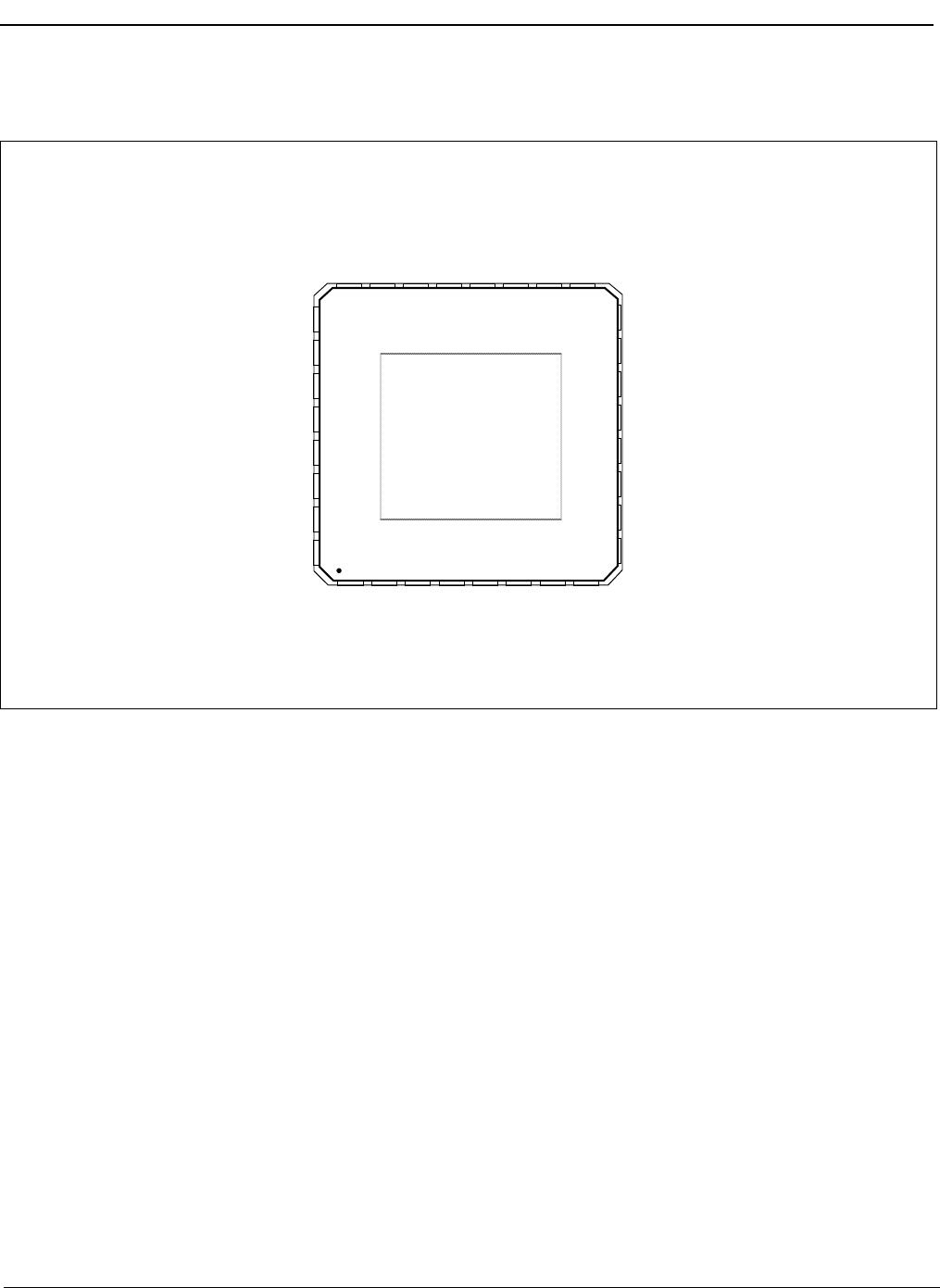
2.0 Pin Description
Pin # Name Description
1, 4,
5, 8
clk0_p, clk0_n,
clk1_p, clk1_n
Differential Input (Analog Input). Differential (or singled ended) input signals. For all
input signal configuration see Section 3.1, “Clock Inputs“.
2, 6 vt0, vt1 On-Chip Input Termination Node (Analog). Center tap between internal 50 Ohm
termination resistors.
For a DC coupled LVPECL input connect this pin through a resistor to ground; 50 Ohms
for 3.3V LVPECL or 20 Ohms for 2.5V LVPECL.
For a DC coupled LVDS input or for an AC coupled differential input, leave this pin
unconnected.
3, 7 ctrl0, ctrl1 Digital Control for On-Chip Input Termination (Input). Selects differential input mode;
0: DC coupled LVPECL or LVDS modes
1: AC coupled differential modes
These pins are internally pulled down to GND.
29, 28,
27, 26,
22, 21,
20, 19,
15, 14,
13, 12
out0_p, out0_n
out1_p, out1_n
out2_p, out2_n
out3_p, out3_n
out4_p, out4_n
out5_p, out5_n
Differential Output (Analog Output). Differential outputs.
11, 16,
18, 23,
25, 30
vdd Positive Supply Voltage. 2.5V
DC
or 3.3 V
DC
nominal.
9, 17,
24, 32
gnd Ground. 0 V.
31 sel Input Select (Input). Selects the reference input that is buffered;
0: clk0
1: clk1
This pin is internally pulled down to GND.
10 NC No Connection. Leave unconnected.