LT1209CN#PBF

1
LT1208/LT1209
Dual and Quad
45MHz, 400V/µs Op Amps
45MHz Gain-Bandwidth
400V/µs Slew Rate
Unity-Gain Stable
7V/mV DC Gain, R
L
= 500
3mV Maximum Input Offset Voltage
±12V Minimum Output Swing into 500
Wide Supply Range: ±2.5V to ±15V
7mA Supply Current per Amplifier
90ns Settling Time to 0.1%, 10V Step
Drives All Capacitive Loads
D
U
ESCRIPTIO
S
F
EA
T
U
RE
The LT1208/LT1209 are dual and quad very high speed
operational amplifiers with excellent DC performance. The
LT1208/LT1209 feature reduced input offset voltage and
higher DC gain than devices with comparable bandwidth
and slew rate. Each amplifier is a single gain stage with
outstanding settling characteristics. The fast settling time
makes the circuit an ideal choice for data acquisition
systems. Each output is capable of driving a 500 load to
±12V with ±15V supplies and a 150 load to ±3V on ±5V
supplies. The amplifiers are also capable of driving large
capacitive loads which make them useful in buffer or cable
driver applications.
The LT1208/LT1209 are members of a family of fast, high
performance amplifiers that employ Linear Technology
Corporation’s advanced bipolar complementary
processing.
U
A
O
PP
L
IC
AT
ITY
P
I
CA
L
U
S
A
O
PP
L
IC
AT
I
Wideband Amplifiers
Buffers
Active Filters
Video and RF Amplification
Cable Drivers
Data Acquisition Systems
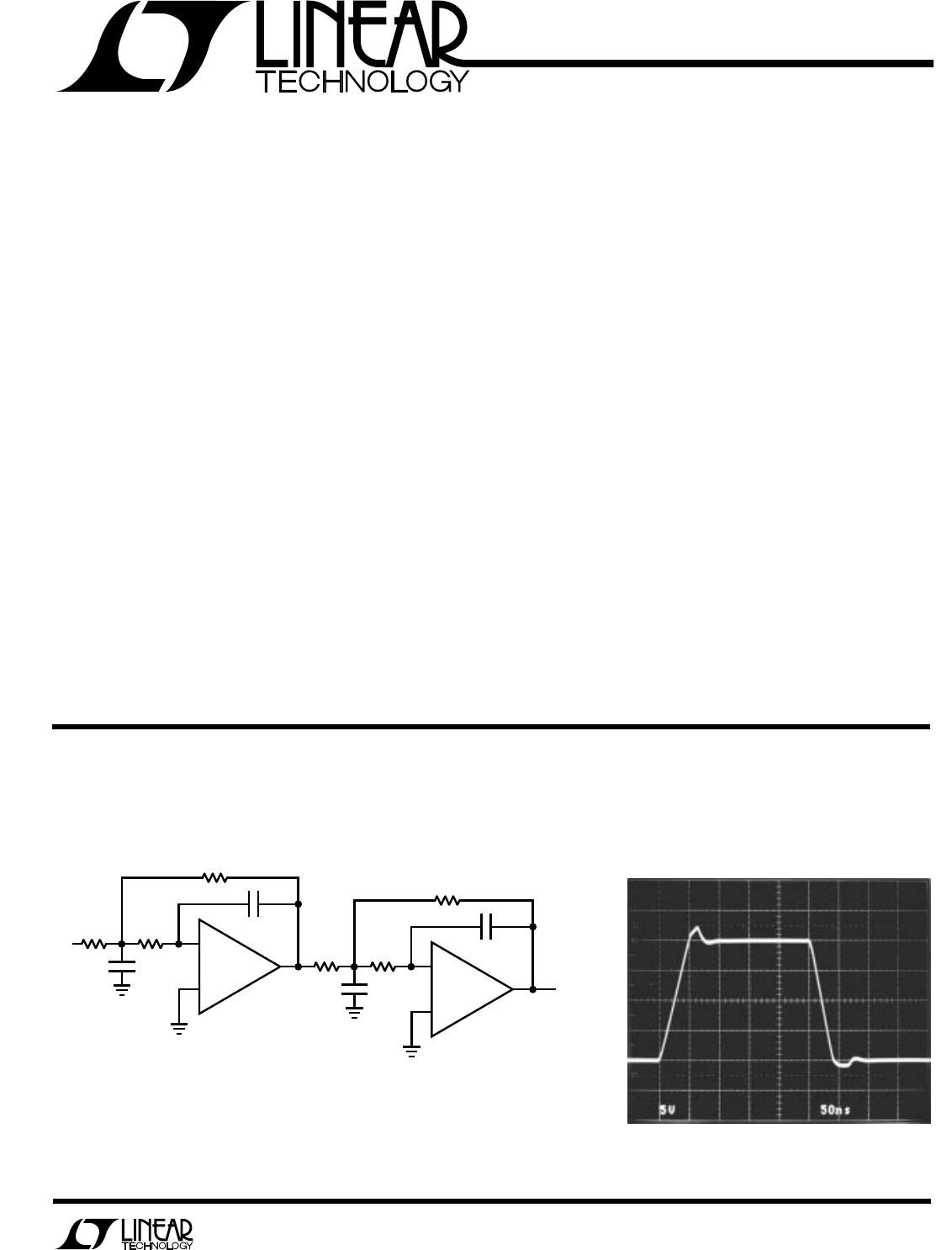
1MHz, 4th Order Butterworth Filter
1208/09 TA02
+
1/2
LT1208
2.67k909
47pF
220pF
V
IN
909
+
1/2
LT1208
2.21k1.1k
22pF
470pF
1.1k
V
OUT
1208/09 TA01
Inverter Pulse Response
LT1208/LT1209
2
A
U
G
W
A
W
U
W
ARB
S
O
LU
T
EXI T
I
S
Total Supply Voltage (V
+
to V
).............................. 36V
Differential Input Voltage ........................................ ±6V
Input Voltage ........................................................... ±V
S
Output Short-Circuit Duration (Note 1)........... Indefinite
Operating Temperature Range
LT1208C/LT1209C .......................... 40°C to 85°C
Maximum Junction Temperature
Plastic Package ............................................. 150°C
Storage Temperature Range ................ – 65°C to 150°C
Lead Temperature (Soldering, 10 sec)................. 300°C
WU
U
PACKAGE
/
O
RDER I FOR ATIO
ORDER PART
NUMBER
ORDER PART
NUMBER
LT1208CS8
S8 PART MARKING
1208
1
2
3
4
8
7
6
5
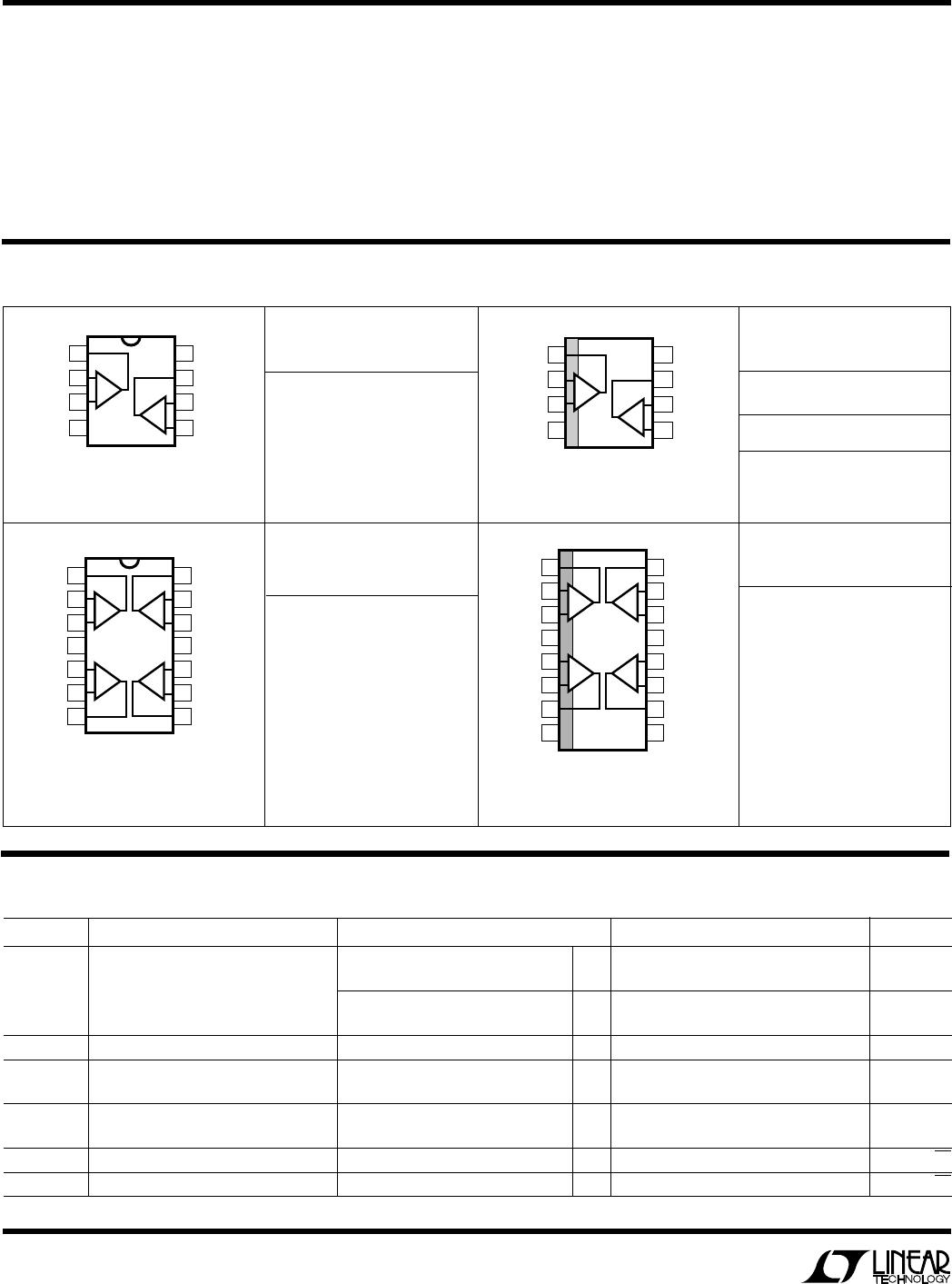
TOP VIEW
OUT A
IN A
+IN A
V
V
+
OUT B
IN B
+IN B
N8 PACKAGE
8-LEAD PLASTIC DIP
A
B
T
JMAX
= 150°C, θ
JA
= 150°C/W
T
JMAX
= 150°C, θ
JA
= 100°C/W
ORDER PART
NUMBER
ORDER PART
NUMBER
LT1209CS
LT1209CN
T
JMAX
= 150°C, θ
JA
= 100°C/W
T
JMAX
= 150°C, θ
JA
= 70°C/W
E
LECTR
IC
AL C CHARA TERIST
ICS
V
S
= ±15V, T
A
= 25°C, R
L
= 1k, V
CM
= 0V, unless otherwise noted.
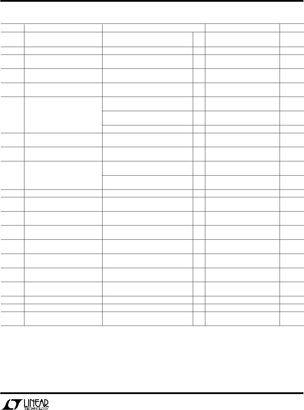
SYMBOL PARAMETER CONDITIONS MIN TYP MAX UNITS
V
OS
Input Offset Voltage V
S
= ±5V (Note 2) 0.5 3.0 mV
0°C to 70°C 4.0 mV
V
S
= ±15V (Note 2) 1.0 5.0 mV
0°C to 70°C 6.0 mV
Input V
OS
Drift 25 µV/°C
I
OS
Input Offset Current V
S
= ±5V and V
S
= ±15V 100 400 nA
0°C to 70°C 600 nA
I
B
Input Bias Current V
S
= ±5V and V
S
= ±15V 4 8 µA
0°C to 70°C 9 µA
e
n
Input Noise Voltage f = 10kHz 22 nV/Hz
i
n
Input Noise Current f = 10kHz 1.1 pA/Hz
1
2
3
4
5
6
7
TOP VIEW
N PACKAGE
14-LEAD PLASTIC DIP
14
13
12
11
10
9
8
A
D
OUT A
IN A
+IN A
V
+
+IN B
IN B
OUT B
OUT D
IN D
+IN D
V
–
+IN C
IN C
OUT C
CB
1
2
3
4
8
7
6
5
TOP VIEW
S8 PACKAGE
8-LEAD PLASTIC SOIC
A
B
OUT A
IN A
+IN A
V
V
+
OUT B
IN B
+IN B
TOP VIEW
S PACKAGE
16-LEAD PLASTIC SOIC
1
2
3
4
5
6
7
8
16
15
14
13
12
11
10
9
A
D
OUT A
IN A
+IN A
V
+
+IN B
IN B
OUT B
NC
OUT D
IN D
+IN D
V
–
+IN C
IN C
OUT C
NC
CB
LT1208CN8
CONTACT FACTORY FOR
MILITARY/883B PARTS
3
LT1208/LT1209
E
LECTR
IC
AL C CHARA TERIST
ICS
V
S
= ±15V, T
A
= 25°C, R
L
= 1k, V
CM
= 0V, unless otherwise noted.
SYMBOL PARAMETER CONDITIONS MIN TYP MAX UNITS
R
IN
Input Resistance V
CM
= ±12V 20 40 M
Differential 250 k
C
IN
Input Capacitance 2pF
CMRR Common-Mode Rejection Ratio V
S
= ±15V, V
CM
= ±12V; V
S
= ±5V, 86 98 dB
V
CM
= ±2.5V, 0°C to 70°C 83 dB
PSRR Power Supply Rejection Ratio V
S
= ±5V to ±15V 76 84 dB
0°C to 70°C 75 dB
Input Voltage Range V
S
= ±15V ±12 ±13 V
V
S
= ±5V ±2.5 ±3V
A
VOL
Large-Signal Voltage Gain V
S
= ±15V, V
OUT
= ±10V, R
L
= 500 3.3 7 V/mV
0°C to 70°C 2.5 V/mV
V
S
= ±5V, V
OUT
= ±2.5V, R
L
= 500 2.5 7 V/mV
0°C to 70°C 2.0 V/mV
V
S
= ±5V, V
OUT
= ±2.5V, R
L
= 150 3 V/mV
V
OUT
Output Swing V
S
= ±15V, R
L
= 500, 0°C to 70°C 12.0 13.3 ±V
V
S
= ±5V, R
L
= 150, 0°C to 70°C 3.0 3.3 ±V
I
OUT
Output Current V
S
= ±15V, V
OUT
= ±12V, 0°C to 70°C 24 40 mA
V
S
= ±5V, V
OUT
= ±3V, 0°C to 70°C 20 40 mA
SR Slew Rate V
S
= ±15V, A
VCL
= –2, (Note 3) 250 400 V/µs
0°C to 70°C 200 V/µs
V
S
= ±5V, A
VCL
= –2, (Note 3) 150 250 V/µs
0°C to 70°C 130 V/µs
Full Power Bandwidth 10V Peak, (Note 4) 6.4 MHz
GBW Gain-Bandwidth V
S
= ±15V, f = 1MHz 45 MHz
V
S
= ±5V, f = 1MHz 34 MHz
t
r
, t
f
Rise Time, Fall Time V
S
= ±15V, A
VCL
= 1, 10% to 90%, 0.1V 5 ns
V
S
= ±5V, A
VCL
= 1, 10% to 90%, 0.1V 7 ns
Overshoot V
S
= ±15V, A
VCL
= 1, 0.1V 30 %
V
S
= ±5V, A
VCL
= 1, 0.1V 20 %
Propagation Delay V
S
= ±15V, 50% V
IN
to 50%V
OUT
5ns
V
S
= ±5V, 50% V
IN
to 50%V
OUT
7ns
t
s
Settling Time V
S
= ±15V, 10V Step, V
S
= ±5V, 90 ns
5V Step, 0.1%
Differential Gain f = 3.58MHz, R
L
= 150 1.30 %
f = 3.58MHz, R
L
= 1k 0.09 %
Differential Phase f = 3.58MHz, R
L
= 150 1.8 Deg
f = 3.58MHz, R
L
= 1k 0.1 Deg
R
O
Output Resistance A
VCL
= 1, f = 1MHz 2.5
Crosstalk V
OUT
= ±10V, R
L
= 500 100 94 dB
I
S
Supply Current Each Amplifier, V
S
= ±5V and V
S
= ±15V 7 9 mA
0°C to 70°C 10.5 mA
Note 3: Slew rate is measured in a gain of –2. For ±15V supplies measure
between ±10V on the output with ±6V on the input. For ±5V supplies
measure between ±2V on the output with ±1.75V on the input.
Note 4: Full power bandwidth is calculated from the slew rate
measurement: FPBW = SR/2πV
P
.
The
denotes the specifications which apply over the full operating
temperature range.
Note 1: A heat sink may be required to keep the junction temperature
below absolute maximum when the output is shorted indefinitely.
Note 2: Input offset voltage is tested with automated test equipment and is
exclusive of warm-up drift.
LT1209CN#PBF

Mfr. #:
Manufacturer:
Analog Devices Inc.
Description:
High Speed Operational Amplifiers 250V/us Hi Speed Quad Op Amp
Lifecycle:
New from this manufacturer.
Delivery:
DHL FedEx Ups TNT EMS
Payment:
T/T Paypal Visa MoneyGram Western Union