LT1208/LT1209
8
U
S
A
O
PP
L
IC
AT
I
WU
U
I FOR ATIO
Low Voltage Operation
The LT1208/LT1209 are functional at room temperature
with only 3V of total supply voltage. Under this condition,
however, the undistorted output swing is only 0.8V
P-P
. A
more realistic condition is operation at ±2.5V supplies (or
5V and ground). Under these conditions, at room tem-
perature, the typical input common-mode range is 1.9V to
–1.3V (for a V
OS
change of 1mV), and a 5MHz, 2V
P-P
sine
wave can be faithfully reproduced. With 5V total supply
voltage the gain-bandwidth is reduced to 26MHz and the
slew rate is reduced to 135V/µs.
Power Dissipation
The LT1208/LT1209 combine high speed and large output
current drive in small packages. Because of the wide
supply voltage range, it is possible to exceed the maxi-
mum junction temperature under certain conditions.
Maximum junction temperature (T
J
) is calculated from the
ambient temperature (T
A
) and power dissipation (P
D
) as
follows:
LT1208CN8: T
J
= T
A
+ (P
D
× 100°C/W)
LT1208CS8: T
J
= T
A
+ (P
D
× 150°C/W)
LT1209CN: T
J
= T
A
+ (P
D
× 70°C/W)
LT1209CS: T
J
= T
A
+ (P
D
× 100°C/W)
Maximum power dissipation occurs at the maximum
supply current and when the output voltage is at 1/2 of
either supply voltage (or the maximum swing if less than
1/2 supply voltage).
For each amplifier P
DMAX
is as follows:
Example: LT1208 in S8 at 70°C, V
S
= ±10V, R
L
= 500Ω
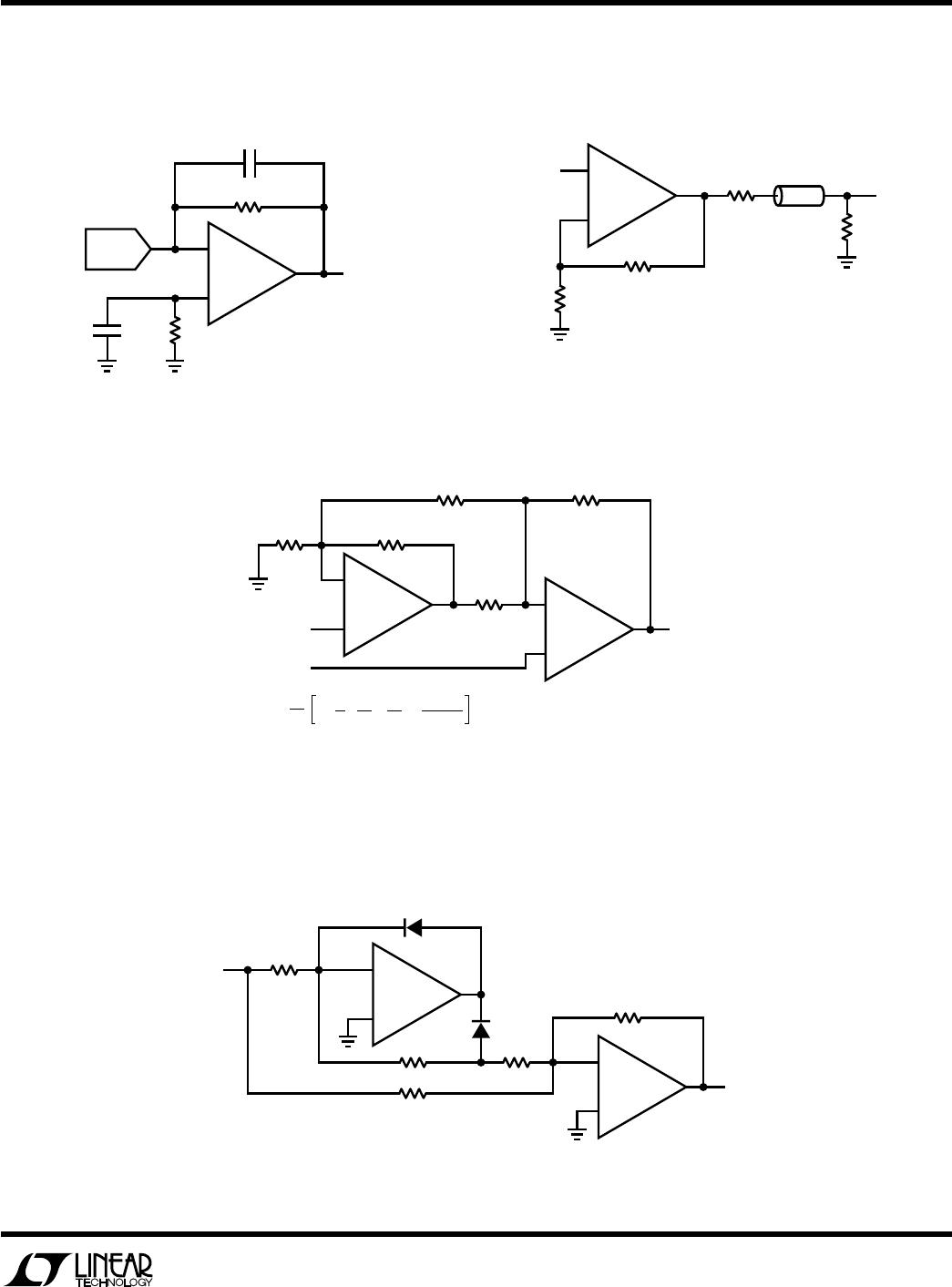
DAC Current-to-Voltage Converter
The wide bandwidth, high slew rate and fast settling time
of the LT1208/LT1209 make them well-suited for current-
to-voltage conversion after current output D/A converters.
A typical application with a DAC-08 type converter (full-
scale output of 2mA) uses a 5k feedback resistor. A 7pF
compensation capacitor across the feedback resistor is
used to null the pole at the inverting input caused by the
DAC output capacitance. The combination of the LT1208/
LT1209 and DAC settles to less than 40mV (1LSB) in
140ns for a 10V step.
Large-Signal Transient Response
A
V
= 1 1208/09 AI04
A
V
= –1 1208/09 AI06
Large-Signal Transient Response
P
DMAX
= (V
+
– V
–
)(I
SMAX
) +
(0.5V
+
)
2
R
L
P
DMAX
= (20V)(10.5mA) + = 260mW
(5V)
2
500Ω
T
J
= 70°C + (2 × 260mW)(150°C/W) = 148°C