PCF8563 All information provided in this document is subject to legal disclaimers. © NXP Semiconductors N.V. 2015. All rights reserved.
Product data sheet Rev. 11 — 26 October 2015 28 of 45
NXP Semiconductors
PCF8563
Real-time clock/calendar
12. Static characteristics
Table 29. Static characteristics
V
DD
= 1.8 V to 5.5 V; V
SS
=0V; T
amb
=
40
C to +85
C; f
osc
= 32.768 kHz; quartz R
s
=40k
; C
L
= 8 pF; unless otherwise
specified.
Symbol Parameter Conditions Min Typ Max Unit
Supplies
V
DD
supply voltage interface inactive;
f
SCL
=0Hz;
T
amb
=25C
[1]
1.0 - 5.5 V
interface active;
f
SCL
= 400 kHz
1.8 - 5.5 V
clock data integrity;
T
amb
=25C
V
low
-5.5V
I
DD
supply current interface active
f
SCL
=400kHz --800A
f
SCL
=100kHz --200A
interface inactive (f
SCL
= 0 Hz); CLKOUT
disabled; T
amb
=25C
[2]
V
DD
= 5.0 V - 275 550 nA
V
DD
= 3.0 V - 250 500 nA
V
DD
= 2.0 V - 225 450 nA
interface inactive (f
SCL
= 0 Hz); CLKOUT
disabled; T
amb
= 40 Cto +85C
[2]
V
DD
= 5.0 V - 500 750 nA
V
DD
= 3.0 V - 400 650 nA
V
DD
= 2.0 V - 400 600 nA
interface inactive (f
SCL
= 0 Hz); CLKOUT
enabled at 32 kHz; T
amb
=25C
[2]
V
DD
= 5.0 V - 825 1600 nA
V
DD
= 3.0 V - 550 1000 nA
V
DD
= 2.0 V - 425 800 nA
interface inactive (f
SCL
= 0 Hz); CLKOUT
enabled at 32 kHz; T
amb
= 40 Cto +85C
[2]
V
DD
= 5.0 V - 950 1700 nA
V
DD
= 3.0 V - 650 1100 nA
V
DD
= 2.0 V - 500 900 nA
Inputs
V
IL
LOW-level input
voltage
0.5 - +0.3V
DD
V
V
IH
HIGH-level
input voltage
0.7V
DD
-5.5V
I
LI
input leakage
current
V
I
=V
DD
or V
SS
10 +1A
C
i
input
capacitance
[3]
--7pF
PCF8563 All information provided in this document is subject to legal disclaimers. © NXP Semiconductors N.V. 2015. All rights reserved.
Product data sheet Rev. 11 — 26 October 2015 29 of 45
NXP Semiconductors
PCF8563
Real-time clock/calendar
[1] For reliable oscillator start-up at power on use V
DD
greater than 1.3 V. If powered up at 1.0 V the oscillator will start but it might be a bit
slow, especially if at high temperature. Normally the power supply is not 1.0 V at start up and only comes at the end of battery discharge.
V
DD
min of 1.0 V is specified so that the customer can calculate how large a battery or capacitor they need for their application. V
DD
min
of 1.3 V or greater is needed to ensure speedy oscillator start-up time.
[2] Timer source clock =
1
60
Hz, level of pins SCL and SDA is V
DD
or V
SS
.
[3] Tested on sample basis.
Outputs
I
OL
LOW-level
output current
output sink current;
V
OL
=0.4V; V
DD
=5V
on pin SDA 3 - - mA
on pin INT
1- - mA
on pin CLKOUT 1 - - mA
I
LO
output leakage
current
V
O
=V
DD
or V
SS
10 +1A
Voltage detector
V
low
low voltage T
amb
=25C; sets bit VL; see Figure 6 -0.91.0V
Table 29. Static characteristics
…continued
V
DD
= 1.8 V to 5.5 V; V
SS
=0V; T
amb
=
40
C to +85
C; f
osc
= 32.768 kHz; quartz R
s
=40k
; C
L
= 8 pF; unless otherwise
specified.
Symbol Parameter Conditions Min Typ Max Unit
T
amb
=25C; Timer = 1 minute. T
amb
=25C; Timer = 1 minute.
Fig 23. Supply current I
DD
as a function of supply
voltage V
DD
; CLKOUT disabled
Fig 24. Supply current I
DD
as a function of supply
voltage V
DD
; CLKOUT = 32 kHz
02 6
mgr888
4
V
DD
(V)
1
0
0.4
0.2
0.8
0.6
I
DD
(μA)
02 6
mgr889
4
V
DD
(V)
1
0
0.4
0.2
0.8
0.6
I
DD
(μA)
PCF8563 All information provided in this document is subject to legal disclaimers. © NXP Semiconductors N.V. 2015. All rights reserved.
Product data sheet Rev. 11 — 26 October 2015 30 of 45
NXP Semiconductors
PCF8563
Real-time clock/calendar
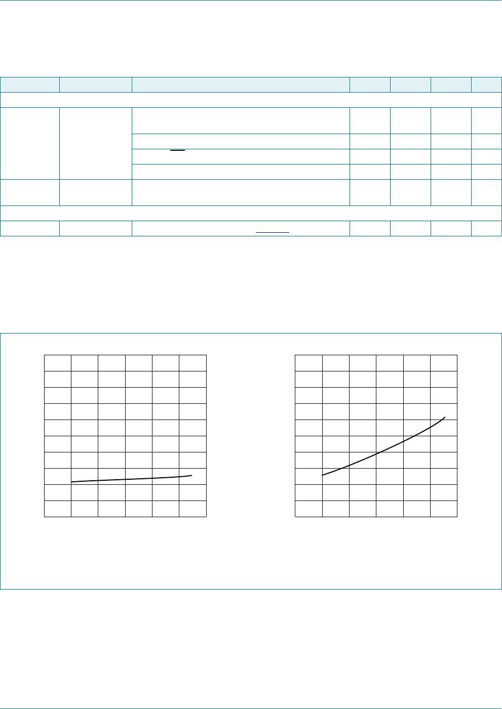
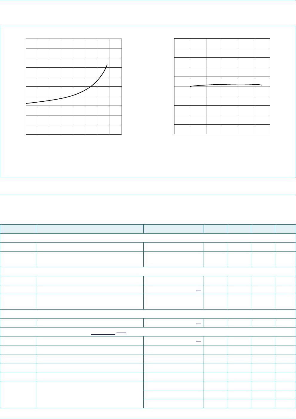
13. Dynamic characteristics
V
DD
= 3 V; Timer = 1 minute. T
amb
=25C; normalized to V
DD
=3V.
Fig 25. Supply current I
DD
as a function of
temperature T; CLKOUT = 32 kHz
Fig 26. Frequency deviation as a function of supply
voltage V
DD
40 0 40 120
mgr890
80
T (°C)
1
0
0.4
0.2
0.8
0.6
I
DD
(μA)
02 6
4
2
4
2
0
mgr891
4
V
DD
(V)
frequency
deviation
(ppm)
Table 30. Dynamic characteristics
V
DD
= 1.8 V to 5.5 V; V
SS
=0V; T
amb
=
40
C to +85
C; f
osc
= 32.768 kHz; quartz R
s
=40k
; C
L
= 8 pF; unless otherwise
specified.
Symbol Parameter Conditions Min Typ Max Unit
Oscillator
C
OSCO
capacitance on pin OSCO 15 25 35 pF
f
osc
/f
osc
relative oscillator frequency variation V
DD
=200mV;
T
amb
=25C
-0.2-ppm
Quartz crystal parameters (f = 32.768 kHz)
R
s
series resistance - - 100 k
C
L
load capacitance parallel
[1]
7 - 12.5 pF
C
trim
trimmer capacitance external;
on pin OSCI
5- 25pF
CLKOUT output
CLKOUT
duty cycle on pin CLKOUT
[2]
-50-%
I
2
C-bus timing characteristics (see Figure 27)
[3][4]
f
SCL
SCL clock frequency
[5]
- - 400 kHz
t
HD;STA
hold time (repeated) START condition 0.6 - - s
t
SU;STA
set-up time for a repeated START condition 0.6 - - s
t
LOW
LOW period of the SCL clock 1.3 - - s
t
HIGH
HIGH period of the SCL clock 0.6 - - s
t
r
rise time of both SDA and SCL signals
standard-mode - - 1 s
fast-mode - - 0.3 s

PCF8563T/5,518

Mfr. #:
Manufacturer:
NXP Semiconductors
Description:
Real Time Clock Binary I2C 1-5V RTC IC
Lifecycle:
New from this manufacturer.
Delivery:
DHL FedEx Ups TNT EMS
Payment:
T/T Paypal Visa MoneyGram Western Union