AD22057RZ

AD22057
–6–
REV. A
To produce a full-scale output of +4 V, a gain ×40 is used, adjust-
able by ±5% to absorb the tolerance in the sense resistor. There is
sufficient headroom to allow at least a 10% overrange (to +4.4 V).
The roughly triangular voltage across the sense resistor is aver-
aged by a single-pole low-pass filter, here set with a corner fre-
quency of f
C
= 3.6 Hz, which provides about 30 dB of attenuation
at 100 Hz. A higher rate of attenuation can be obtained by a
two-pole filter having f
C
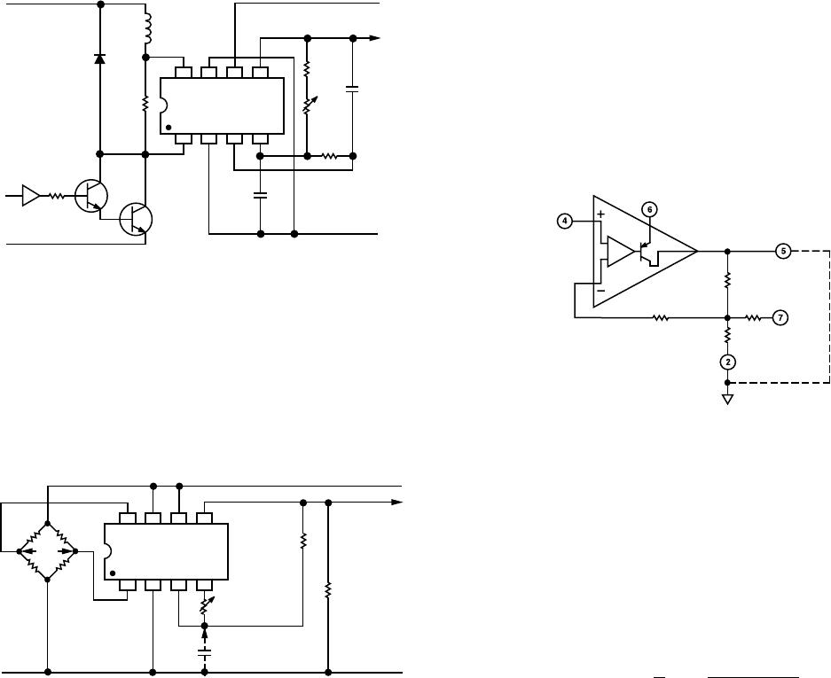
= 20 Hz, as shown in Figure 11. Al-
though this circuit uses two separate capacitors, the total capaci-
tance is less than half that needed for the single-pole filter.
AD22057
+IN OFS +V
S
OUT
–IN
GND A1 A2
100mV
SOLENOID
LOAD
POWER
DARLINGTON
CMOS DRIVER
+V
S
(BATTERY)
CHASSIS
C
432kV
50kV
+5V
ANALOG
OUTPUT
CORNER FREQUENCY
= 1Hz-mF
(0.05mF FOR f
C
= 20Hz)
ANALOG
COMMON
FLYBACK
DIODE
127kV
C
Figure 11. Illustration of Two-Pole Low-Pass Filtering
STRAIN GAGE INTERFACE: MIDSCALE OFFSET
FEATURE
The AD22057 can be used to interface a strain gage to a subse-
quent process where only a single supply voltage is available. In
this application, the midscale offset feature is valuable, since the
output of the bridge may have either polarity. Figure 12 shows
typical connections.
AD22057
+IN OFS +V
S
OUT
–IN GND A1 A2
R
L
10kV
+V
S
ANALOG OUTPUT
ANALOG COMMON
100kV
V
OS
NULL
OPTIONAL
LP FILTER
125kV
(SETS GAIN
TO 3 100)
V
G
R
R
R
R
Figure 12. Typical Connections for a Strain Gage Interface
Using the Offset Feature
The offset is obtained by connecting Pin 7 (OFS) to the supply
voltage. In this way, the output of the AD22057 is centered to
midway between the supply and ground. In many systems the
supply will also serve as the reference voltage for a subsequent
A/D converter. Alternatively, Pin 7 may be tied to the reference
voltage from an independent source. The AD22057 is trimmed
to guarantee an accuracy of ±2% on the 0.5 ratio between the
voltage on Pin 7 and the output.
An ac excitation of up to ±2 V can also be used because the
common-mode range of the AD22057 extends to –1 V. Assum-
ing a full-scale bridge output (V
G
) of ±10 mV, a gain of ×100
might be used to provide an output of ±1 V (a full-scale range
of +1.5 V to +3.5 V). This gain is achieved using the method
discussed in connection with Figure 5. Note that the gain-
setting resistor does not affect the accuracy of the midscale
offset. (However, if the gain were lowered, using a resistor to
ground, this offset would no longer be accurate.) A V
OS
nulling
pot is included for illustrative purposes. One-, two- and three-
pole filtering can also be implemented, as discussed in the
Low-Pass Filtering section.
Using the Midscale Offset Feature
Figure 13 shows a more detailed schematic of the output am-
plifier A2. Because this is a single supply device, the output
stage has no pull-down transistor. Such a transistor would limit
the minimum output to several hundred millivolts above
ground. When using the AD22057 in unipolar mode (Pin 7
grounded), the resistors making up the feedback network also
act as a pull-down for the output stage.
A2
10kV
95kV
+V
S
20kV
OFS
OUT
20kV
R
L
GND
Figure 13. Detailed Schematic of Output Amplifier A2
If the output is called upon to source current (not sink), then it
can swing almost completely to ground (within 20 mV). How-
ever, if the offset pin is connected to some positive voltage
source, this source will “pull up” the output voltage, thereby
limiting the minimum output swing. With no external load the
minimum output voltage possible is V
OFS
/2. For example, if Pin
7 is connected to +5 V, the minimum output voltage is equal
to the offset voltage of 2.5 V. By adding an additional load, as
shown, the output swing toward ground can be extended.
The relationship is described by:
V
OUT
>
1
2
V
OFS
R
L
R
L
+20k*
*This 20 k resistor is internal to the AD22057 and can vary by ±30%.
where R
L
is an externally applied load resistor. However, R
L
cannot be made arbitrarily small since this would require exces-
sive current from the output. The output current should be
limited to 5 mA total.
AD22057
–7–
REV. A
APPLICATION HINTS
Frequency Compensation
As are all closed-loop op amp circuits, the AD22057 is sensitive
to capacitive loading at its output. However, the AD22057 is
sensitive at higher output voltages due to nonlinear effects in
the rail-to-rail design of the buffer amplifier (A2). In this
amplifier the output stage gain increases with increasing output
voltage. This behavior does not affect dc parameters such as
gain accuracy or linearity; however, it can compromise ac sta-
bility. When operating from a power supply of 5 V or less (and,
therefore, V
OUT
< 5 V), the AD22057 can drive capacitive
loads up to 25 pF with no external components. When operat-
ing at higher supply voltages (which are associated with higher
output voltages) and/or driving larger capacitive loads, an exter-
nal compensation network should be used. Figure 14 shows an
R-C “snubber” circuit loading the output of the AD22057.
This combination, in conjunction with the internal 20 k resis-
tance, forms a lag network. This network attenuates the open-
loop gain of the amplifier at higher frequencies. The ratio of
R
LAG
to the load seen by the AD22057 determines the high
frequency attenuation seen by the op amp. If R
LAG
is made
1/20th of the total load resistance (20 kR
L
), then 26 dB of
attenuation is obtained at higher frequencies. The capacitor
(C
LAG
) is used to control the frequency of the compensation
network. It should be set to form a 5 µs time constant with the
resistor (R
LAG
). Table I shows the recommended values of
R
LAG
and C
LAG
for various values of external load resistor R
L
.
Ten percent tolerance on these components is acceptable.
Alternatively, the signal may be taken from the midpoint of
R
LAG
–C
LAG
. This output is particularly useful when driving
CMOS analog-to-digital converters. For more information see
the section Driving Charged Redistributed A/D Converters.
Note that when implementing this network large signal re-
sponse is compromised. This occurs because there is no active
pull-down and the lag capacitor must discharge through the
internal feedback resistor (20 k) giving a fairly long-time
constant. For example if C
LAG
= 0.01 µF, the large signal
negative slew characteristic is a decaying exponential with a
time constant of 200 µs.
Table I. Compensation Components vs. External Load
Resistor
R
L
R
LAG
C
LAG
>100 k 470 0.01 µF
> 50 k 390 0.01 µF
> 20 k 270 0.047 µF
> 10 k 200 0.047 µF
> 5 k 100 0.1 µF
> 2 k 47 0.22 µF
Driving Charge Redistribution A/D Converters
When driving CMOS ADCs, such as those embedded in popu-
lar microcontrollers, the charge injection (Q) can cause a
significant deflection in the AD22057 output voltage. Though
generally of short duration, this deflection may persist until
after the sample period of the ADC has expired. It is due to the
relatively high open-loop output impedance of the AD22057.
The effect can be significantly reduced by including the same
R-C network recommended for improving stability (see Fre-
quency Compensation section). The large capacitor in the lag
network helps to absorb the additional charge, effectively lower-
ing the high frequency output impedance of the AD22057. For
these applications the output signal should be taken from the
midpoint of the R
LAG
–C
LAG
combination as shown in Figure 15.
Since the perturbations from the analog-to-digital converter are
small, the output of the AD22057 will appear to be a low
impedance. The transient response will, therefore, have a
time constant governed by the product of the two lag compo-
nents, C
LAG
× R
LAG
. For the values shown in Figure 15, this
time constant is programmed at approximately 10 µs. There-
fore, if samples are taken at several tens of microseconds or more,
there will be negligible “stacking up” of the charge injections.
Figure 14. Using an R-C Network for Compensation
0.01mF
1kV
10kV
+V
S
10kV
AD22057
A2
mPROCESSOR
A/D
IN
Figure 15. Recommended Circuit for Driving CMOS A/D
Converters
UNDERSTANDING THE AD22057
Figure 16 shows the main elements of the AD22057. The signal
inputs at Pins 1 and 8 are first applied to dual resistive attenua-
tors R1 through R4, whose purpose is to reduce the common-
mode voltage at the input to the preamplifier. The attenuated
signal is then applied to a feedback amplifier based on the very
low drift op amp, A1. The differential voltage across the inputs
is accurately amplified in the presence of common-mode volt-
ages of many times the supply voltage. The overall common-
mode response is minimized by precise laser trimming of R3
and R4, giving the AD22057 a common-mode rejection ratio
(CMRR) of at least 80 dB (10,000:1).
The common-mode range of A1 extends from slightly below
ground to 1 V below +V
S
(at the minimum temperature of
–40°C). Since an attenuation ratio of about 6 is used, the input
common-mode range is –1 V to +24 V using a +5 V supply.
Small filter capacitors C1 and C2 are included to minimize the
effects of spurious RF signals at the inputs, which might cause
dc errors due to the rectification effects at the input to A1. At
high frequencies, even a small imbalance in these components
would seriously degrade the CMRR, so a special high frequency
trim is also carried out during manufacture.
AD22057
–8–
REV. A
PRINTED IN U.S.A.
AD22057
A1
A2
+V
S
R12
100kV
A2
C1
5pF
R1
200kV
R18
1kV
A1
R19 1kV
C2
5pF
R4
41kV
R9
10kV
R7
250V
R17
95kV
R15
10kV
OUT
R16
10kV
R14
20kV
R13
20kV
R5
2.6kV
R3
41kV
GND
OFS
R6
250kV
R8
9kV
R2
200kV
R11
2kV
R10
2kV
IN+
IN–
Figure 16. Simplified Schematic of AD22057, Including Component Values
OUTLINE DIMENSIONS
Dimensions shown in inches and (mm).
Plastic SOIC Package
(SO-8)
0.1968 (5.00)
0.1890 (4.80)
8
5
41
0.2440 (6.20)
0.2284 (5.80)
PIN 1
0.1574 (4.00)
0.1497 (3.80)
0.0688 (1.75)
0.0532 (1.35)
SEATING
PLANE
0.0098 (0.25)
0.0040 (0.10)
0.0192 (0.49)
0.0138 (0.35)
0.0500
(1.27)
BSC
0.0098 (0.25)
0.0075 (0.19)
0.0500 (1.27)
0.0160 (0.41)
88
08
0.0196 (0.50)
0.0099 (0.25)
3 458
Plastic Mini-DIP Package
(N-8)
8
14
5
0.430 (10.92)
0.348 (8.84)
0.280 (7.11)
0.240 (6.10)
PIN 1
SEATING
PLANE
0.022 (0.558)
0.014 (0.356)
0.060 (1.52)
0.015 (0.38)
0.210 (5.33)
MAX
0.130
(3.30)
MIN
0.070 (1.77)
0.045 (1.15)
0.100
(2.54)
BSC
0.160 (4.06)
0.115 (2.93)
0.325 (8.25)
0.300 (7.62)
0.015 (0.381)
0.008 (0.204)
0.195 (4.95)
0.115 (2.93)
C2181a–2–4/99
A unique method of feedback around A1, provided by R9 and
R7, sets the closed-loop gain of the preamplifier to ×10 (from
the input pins). The feedback network is balanced by the inclu-
sion of R6 and R8. The small value of R7 results in a more
practical value for R9 (which would have to be 2 M if the
feedback were taken directly to the inputs of A1). R8 is not
directly connected to ground, but to an optional voltage of one
half that is applied to Pin 7 (OFS). It is trimmed to within close
tolerances through R10 and R11. This allows the output of A1
to be offset to midscale, typically +V
S
/2, by tying Pins 6 and 7
together. (For an example of the use of this feature, see Figure
12.) The gain is adjusted by the single resistor R5, which acts
only on the differential signal. More importantly, it also results
in much less feed forward of the common-mode signal to the
output of A1, which, being a single-supply circuit, has no means
of pulling this output down toward ground in those circum-
stances where the common-mode input is very positive while the
net differential signal is small. (The output of A1 is the collector
of a PNP transistor whose emitter is tied to +V
S
.) R16 is specifi-
cally included to alleviate this problem.
The output of the preamplifier is connected to Pin 3 via R12, a
100 k resistor that is trimmed to within ±3%. The inclusion of
R12 allows a low-pass filter to be formed, with an accurate time
constant, by placing a capacitor from Pin 3 to ground. By sepa-
rating the connections at Pins 3 and 4, a two-pole Sallen and
Key filter can be formed (see Low-Pass Filtering section) and
also provides a means for setting the overall gain to values other
than ×20 (see Altering the Gain section).
The output buffer has a gain of ×2, set by the feedback network
around op amp A2, formed by R15 and R13R14. Note that this
gain is not trimmed to a precise value, but may have a tolerance
of ±3% (max). Only the overall gain of A1 and A2 is trimmed to
within ±0.5% by R5. As a consequence, the gain of A1 may be
in error by ±3% (max) as the trim to R5 absorbs the initial error
in the gain of A2. In most applications Pins 3 and 4 are simply
tied together, but the output buffer can be used independently if
desired. The offset voltage of A2 is nulled during manufacture.
R17 is included to minimize the offset due to bias currents. It is
recommended, in applications where A2 is used independently
and the source resistance is less than 100 k, that the necessary
extra resistance should be included.
The output of A2 is the collector of a PNP transistor whose
emitter is tied to +V
S
. The bias current out of the inverting
input of this amplifier generates an offset voltage of about +1 mV
in R13R14, which is passed directly to the output via R15. This
sets the lowest output that can be reached when there is no load
resistor. However, the output can drive a 1 k load to at least
+4.5 V when +V
S
= +5 V. If operation to much lower minimum
voltages is essential, a load resistor can be added externally.

AD22057RZ

Mfr. #:
Manufacturer:
Analog Devices Inc.
Description:
Current Sense Amplifiers IC INTERFACE AMP
Lifecycle:
New from this manufacturer.
Delivery:
DHL FedEx Ups TNT EMS
Payment:
T/T Paypal Visa MoneyGram Western Union

Products related to this Datasheet