_______________Detailed Description
The MAX685 DC-DC converter accepts an input voltage
between +2.7V and +5.5V and generates both a positive
and negative voltage, using a single inductor (Figure 1).
It alternates between acting as a step-up converter and
as an inverting converter on a cycle-by-cycle basis. Both
output voltages are independently regulated.
Each output is separately controlled by a pulse-width-
modulated (PWM) current mode regulator. This allows
the part to operate at a fixed frequency for use in noise-
sensitive applications. An internal oscillator runs at
220kHz or 400kHz, or can be synchronized to an exter-
nal signal. Since switching alternates between the two
regulators, each operates at half the oscillator frequency
(110kHz, 200kHz, or half the sync frequency). The oscil-
lator can be synchronized to a 200kHz to 480kHz clock.
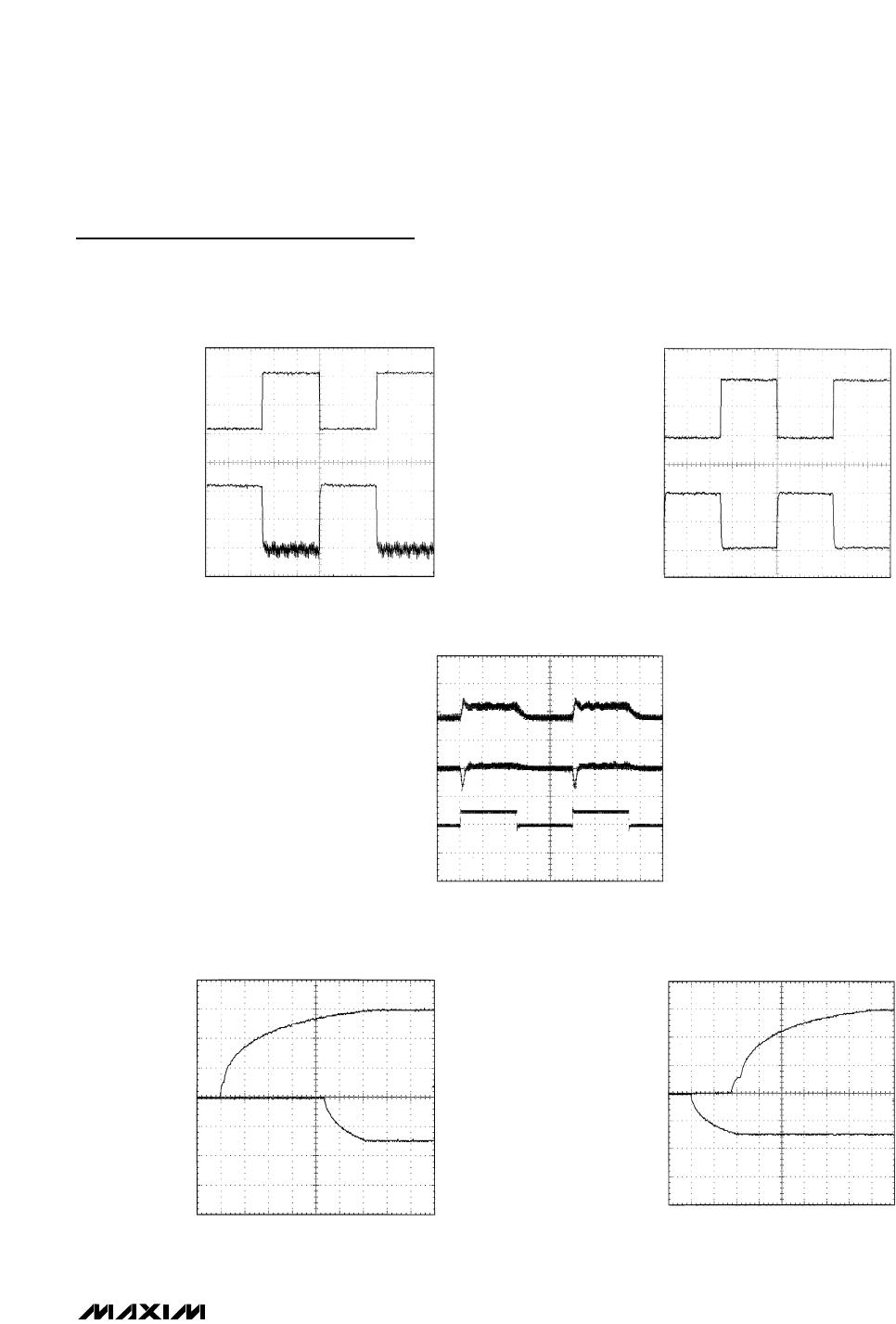
On the first cycle of operation, the part operates as a
step-up converter. LXP connects to V
DD
, LXN pulls to
ground, and the inductor current rises. Once the induc-
tor current rises to a level set by the positive-side error
amplifier, LXN releases and the inductor current flows
through D2 to the positive output. When the inductor
current drops to zero (which happens each cycle under
normal, discontinuous operation), LXN returns to the
input voltage.
On the second cycle, LXN is held at ground. LXP is
pulled up to the input voltage until the current reaches
the limit set by the negative error amplifier. Then LXP is
released and the inductor current flows through D1 to
the negative output. Once the inductor current reaches
zero, the voltage at LXP returns to ground. The wave-
forms at LXN and LXP are shown in Figure 2 for a typi-
cal pair of cycles.
MAX685
Dual-Output (Positive and Negative),
DC-DC Converter for CCD and LCD
6 _______________________________________________________________________________________
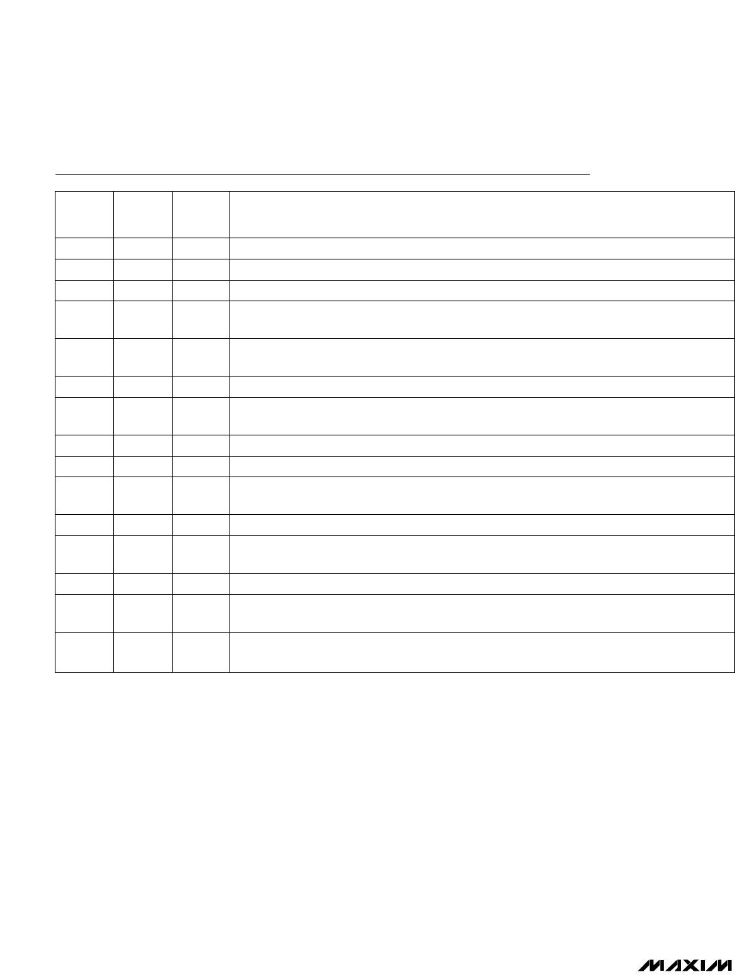
Pin Description
PIN
16-QSOP
P-Channel Switching Inductor Node. LXP turns off when the part enters shutdown.LXP1
FUNCTIONNAME
Internally Connected. Do not externally connect.I.C.2, 15
Open-Drain Power-OK Output. POK is high when both outputs are in regulation. Connect POK
to V
DD
with a 100kΩ pull-up resistor to V
DD
.
POK4
Power Input. Connect to V
DD
.VP3
Shutdown Input. Both outputs go to 0V in shutdown. Connect to V
DD
for automatic startup.
SHDN
6
Supply Input. Bypass V
DD
with a 1.0µF or greater ceramic capacitor to GND.V
DD
8
Sync Input. This pin synchronizes the oscillator to an external clock frequency between 200kHz
and 480kHz. Connect SYNC to GND (220kHz) or V
DD
(400kHz) for internal oscillator frequency.
SYNC7
Power-Up Sequence Select Input. Connect SEQ to GND to power the negative output voltage
first. Connect SEQ to V
DD
to power the positive output first.
SEQ5
GroundGND9
1.25V Reference Voltage Output. Bypass with 0.22µF to GND.REF11
Power Ground. Connect PGND to GND.PGND13, 14
Feedback for the Positive Output Voltage. Connect a resistor-divider between the positive out-
put and GND with the center to FBP to set the positive output voltage.
FBP12
Feedback Input for the Negative Output Voltage. Connect a resistor-divider between the nega-
tive output and REF with the center to FBN to set the negative output voltage.
FBN10
N-Channel Switching Inductor Node. LXN pulls to GND through the internal transistor when the
part is shut down.
LXN16
This pin in not internally connected.N.C.—
19, 24
4
2, 3
6
8
7
5
11
13
15, 16, 17
14
PIN
24-TQFN
12
22, 23
20, 21
1, 9, 10,
18