The current into the LXN pin is sensed to measure the
inductor current. The MAX685 controls the inductor cur-
rent to regulate both the positive and negative output
voltages.
SEQ and Power OK (POK)
The SEQ pin controls the power-up sequence. If SEQ is
low, the positive output is disabled until the negative
output is within 90% of its regulation point. If SEQ is
high, the negative output is disabled until the positive
output is within 90% of its regulation point. The power-
OK output (POK) indicates that both output voltages
are in regulation. When both outputs are within 90% of
their regulation points, POK becomes high impedance.
Should one or both of the output voltages fall below
90% of their regulation points, POK pulls to ground.
POK can sink up to 2mA. To reduce current consump-
tion, POK is high impedance while the part is in shut-
down. When coming out of shutdown, POK remains
high impedance for 50ns (typ) before going low.
Connect POK to V
DD
through a 100k resistor.
Synchronization/Internal
Frequency Selection
The MAX685 operates at a fixed switching frequency.
Set the operating frequency using the SYNC pin. If
SYNC is grounded, the part operates at the internally set
220kHz frequency. When SYNC is connected to V
DD
,
the part operates at 400kHz. The MAX685 can also be
synchronized to signals between 200kHz and 480kHz.
Note that each output switches at half the oscillator or
synchronized frequency. Since the actual switching fre-
quency is one-half the applied clock signal, drive SYNC
at twice the desired switching frequency.
MAX685
Dual-Output (Positive and Negative),
DC-DC Converter for CCD and LCD
_______________________________________________________________________________________ 7
Figure 1. Functional Diagram
NEGATIVE
ERROR
AMP
TO V
OUT-
FBN
FBP
TO V
OUT+
REF
POSITIVE
ERROR
AMP
1.25V
REF
CONTROL
LOGIC
POK VP
V
DD
P
N
PGND
GND
SYNC SEQ SHDN
LXN
D2
D1
V
OUT-
V
OUT+
LXP
MAX685
+15V
+5V
0V
0V
-7.5V
LXN
LXP
Figure 2. LXN and LXP Waveforms (see also Figure 5)
MAX685
Dual-Output (Positive and Negative),
DC-DC Converter for CCD and LCD
8 _______________________________________________________________________________________
Applications Information
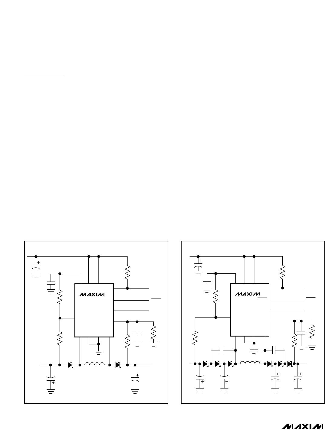
Figure 3 shows the standard application circuit for the
MAX685. The values shown in Table 1 will work well for
output currents up to 10mA. However, this circuit can
be optimized to a particular application by using differ-
ent capacitors and a different inductor.
Higher Output Voltages
If the application requires output voltages greater than
-7.5V or +24V, use the circuit of Figure 4. This circuit
uses a charge pump to increase the output voltage
without increasing the voltage stress on the LX_ pin.
The maximum output voltages of the circuit in Figure 4
are -15V and +48V.
The voltage rating on D2, D5, and D6 must be 30V or
greater. For a larger negative output voltage without a
larger positive output (or vice versa), use one-half of
the Figure 4 circuit with one-half of the Figure 3 circuit.
Inductor Selection
A 22µH inductor is suitable for most applications.
Larger inductances will reduce inductor ripple current
and output voltage ripple, but they also typically require
larger physical size if increased resistance and losses
are not also allowed.
Small inductors are typically preferred because of
compact design and low cost. Murata LHQ and
TDK NLC types are examples of small surface-mount
inductors that work for most applications. Because these
small-size inductors use thinner wire, they exhibit higher
resistance and have greater losses than larger ones. If
the application demands higher efficiency, use larger,
lower resistance coils such as the Sumida CD43 or CD54,
Coilcraft DT1608 or DO1608, or Coiltronics UP1V series.
Filter Capacitor Selection
The output ripple voltage is a function of the peak in-
ductor current, frequency, and type and value of the
output capacitors. Capacitors with low equivalent-
series resistance (ESR) and large capacitance reduce
output ripple. Typically, tantalum or ceramic capacitors
are optimal. Tantalum capacitors have higher ESR and
higher capacitance than ceramic capacitors. Therefore
the ESR of tantalum capacitors determines the output
ripple, because at the frequencies used the ESR domi-
nates the impedance of the capacitor. If ceramic
capacitors are used, the capacitance determines the
output ripple.
MAX685
REF
VP V
DD
LXP
FBN
POK
POK
SHDN
SYNC
C5
47pF
R1
1.0M
R5
100k
D2
MBR0520
L1
22µH
D1
MBR0520
R2
90.9k
+15V
V
OUT+
C4
2.2µF
C3
2.2µF
C2
0.22µF
C1
10µF
V
IN
R3
750k
R4
124k
-7.5V
V
OUT-
SHDN
PGND
LXNGND
SYNC
FBP
Figure 3. Standard Application Circuit
MAX685
REF
VP V
DD
LXP
C6
1µF
C8
1µF
FBN
POK
POK
SHDN
SYNC
C5
47pF
R1
R5
100k
D2
D5
D6
L1
22µH
D3
D4
D1
R2
V
OUT+
C9
2.2µF
C7
2.2µF
C3
2.2µF
C2
0.22µF
C1
10µF
V
IN
R3
R4
V
OUT-
SHDN
PGND
LXNGND
SYNC
FBP
C4
2.2µF
Figure 4. Circuit for Output Voltages < -9V and > +24V
MAX685
Dual-Output (Positive and Negative),
DC-DC Converter for CCD and LCD
_______________________________________________________________________________________ 9
Setting the Output Voltage
The resistor-divider formed by R4 and R3 sets the neg-
ative output voltage; the resistor-divider formed by R1
and R2 sets the positive output voltage. Let R4 be a
value near 100k to set a resistor-divider current of
approximately 10µA. Determine the value of R3 by the
following:
Let R2 be a value near 100k to set a resistor-divider
current of approximately 10µA. Determine the value of
R1 with the following formula:
R1 = R2 x (V
OUT
+ - 1.24V) / 1.24
Damping LX
LXN and LXP may ring at the conclusion of each
switching cycle when the inductor current falls to zero.
Typically the ringing waveform appears only on LX_
and has no effect on output ripple and noise. If LX_
ringing is still objectionable, it may be damped by con-
necting a series RC in parallel with L1. Typically 1k in
series with 100pF provides good damping with only 3%
efficiency degradation. See Figure 5.
RR
V
V
OUT
34
124
.
=
Any manufacturer
0.22µF ceramic
capacitor
C2
Any manufacturer47pF ceramic capC5
Any manufacturer
2.2µF ceramic
capacitor
C3, C4
Murata LHQ4N220J04 or
TDK NLC32522T-220K
22µH, 0.4A
inductor
L1
Motorola MBR0520LT1 (0.5A)
or Central Semiconductor
CMPSH-3
0.1A, 20V
Schottky rectifier
D1, D2
REF
Sprague 595D106X0010A2T or
AVX TAJA106K010R
10µF, 10V
tantalum cap
C1
MANUFACTURER
PART NUMBER
DESCRIPTION
Table 1. Component Values for the
Typical Operating Circuit
Figure 5. LXN and LXP Waveforms with a Series-Connected
1k Resistor and 100pF Capacitor Connected in Parallel with
L1 to Damp Ringing
+15V
+5V
0V
+5V
0V
-7.5V
LXN
LXP
___________________Chip Information
TRANSISTOR COUNT: 902
SUBSTRATE CONNECTED TO GND

MAX685EEE+

Mfr. #:
Manufacturer:
Maxim Integrated
Description:
Switching Voltage Regulators DC/DC Converter for CCD & LCD
Lifecycle:
New from this manufacturer.
Delivery:
DHL FedEx Ups TNT EMS
Payment:
T/T Paypal Visa MoneyGram Western Union

Products related to this Datasheet